Bistability of Nanoscale Ag Islands on a Si(111)-(4×1)-In Surface Induced by Anisotropic Stress
Date:05-11-2009 Print
Understanding the shape evolution of stressed or strained islands during heteroepitaxial growth is of great fundamental interest as well as practical significance in self-assembly of nanostructures, such as quantum dots and quantum wires. One common manifestation is that the growth of a two-dimensional (2D) stressed island, or a 3D strained island with fixed height, displays a spontaneous shape instability: it adopts a compact isotropic shape at small size and an elongated anisotropic shape beyond a critical size, despite the island’s being bounded with isotropic boundary (step) energies and under isotropic stress/strain.
The stress-induced spontaneous shape instability of 2D islands represents a typical case of spontaneous symmetry breaking—transition from a high-symmetry phase to a low-symmetry one, a common phenomenon in nature. (For example, a similar shape transition occurs in carbon nanotubes under pressure.) The original theoretical model as developed by Li, Liu, and Lagally (LLL) has been successfully applied in analyzing various experimental results including equilibrium shape of 2D island, 2D vacancy island, surface adsorption pattern, surface order-disorder phase transition, and elongation of 3D island. One notable feature of the 2D island shape transition, as predicted by the LLL model and confirmed by experiments, is that the transition from the compact isotropic shape to elongated anisotropic shape is a smooth one as the island adopts only one type of shape at a given size. This conventional notion, however, has been recently challenged by Zandvliet and van Gastel (ZG) who predicted a bistability in the stress-induced 2D island shape transition. It was shown that compact isotropic islands may coexist with elongated anisotropic islands in the vicinity of critical size if the island is under anisotropic stress; force monopoles are of opposite directions at neighboring island boundaries. The experimental observation of such bistability, however, is challenging because it usually occurs in a narrow window of surface stress and island boundary energy conditions.
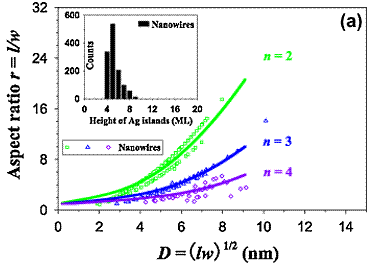
Supported by National Natural Science Foundation and Ministry of Science and Technology of China, Xucun Ma’s group in the Institute of Physics and Condensed Matter Physics National Lab of Chinese Academy of Sciences, cooperated with Qikun Xue’s research team in the Department of Physics of Tsinghua University, studied the stress-induced shape transition of Ag islands on the anisotropic Si(111)-(4×1)-In surface, and experimentally demonstrated the existence of two stability regimes of such islands: a conventional regime at low temperature where only one island shape is stable, and an unconventional regime at room temperature (RT) where isotropic compact islands coexist with anisotropic elongated ones (see Fig.1). Both the statistical analysis of island size and First-principles calculation, collaborated with Prof. Feng Liu at Utah University, confirm that Ag islands are under anisotropic stress, satisfying the prerequisite condition required by ZG model (see Fig.2 and Fig.3).
This work for the first time provides a direct experimental evidence for stress resulted bistability of nanoscale islands on anisotropic surface. They expect such bistability to occur more generally in other systems, and can be exploited for controlling growth of nanostructures on surface.
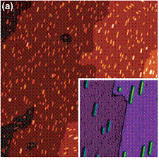 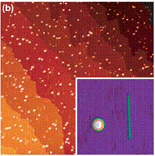 |
| Fig. 1 (a) Large-scale (381×381 nm2) STM image of Ag islands grown on the Si(111)-(4×1)-In surface at LT (145K). Only elongated islands exist. Inset: High resolution STM topography (64×64 nm2) showing details of both Ag nanowires and (4×1)-In surface. (b) Large-scale (1270×1270 nm2) STM image of Ag islands grown on the Si(111)-(4×1)-In surface at RT. Both round and elongated islands exist. Inset: High resolution STM topography (64×64 nm2) of a Ag nanodot and a Ag nanowire. The nanowires in the insets of (a) and (b) occupy two In chains whose period in the transverse direction is 1.33nm. All images were acquired at Vtip = −2.0V , I = 20pA. |
 |
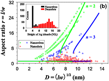 |
| Fig. 2 (a) Dependence of the measured Ag island base aspect ratio (r) on its base size (D) at LT (total 1852 Ag islands are sampled). There are three branches of data points corresponding to the island width of n=2, 3, and 4, respectively. The solid lines are theoretical fit to the data. Inset: The height distributions of Ag nanowires at LT. (b) Same as (a) at RT (total 703 Ag islands are sampled). There are one branch of data of nanodots (r=1) and two branches of data of nanowires correspond to island width n=2 and 3. The solid lines are theoretical fit to the data. Inset: The height distributions of Ag nanodots and nanowires at RT. |
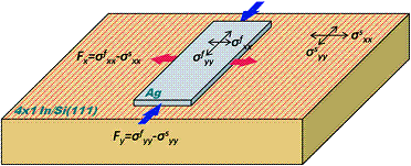 |
| Fig. 3 Schematic illustration of the stress state of a Ag island grown on the Si(111)-(4×1)-In surface. σfand σsdenote the surface stress of the Ag film and In/Si substrate, respectively; F = σf − σsdenotes the force monopoles at the Ag island boundary. |