Molecular Beam Epitaxy Growth, Electronic Properties and Finite-Size Effect of Thin Films of Three-Dimensional Topological Insulators
Date:09-09-2010 Print
Topological insulator (TI) is a new class of quantum matter discovered recently. A TI has a fnite energy gap at Fermi level in its bulk band like a usual insulator, but hosts gapless, spin-filtered, and linearly dispersed surface/boundary states. Not like usual surface/interface states, the surface/interface states of a TI are robust against disorders and impurities since their existence is determined by the topological character of the bulk band. These novel properties make topological insulators turn into the potential materials for low-power electronics and error-tolerant quantum computing, both of which could significantly advance information technology. From the point of view of fundamental condensed matter physics, TI is another system whose physical properties strongly depends on the topological character of its electronic structures, following quantum Hall effect, spin Hall effect, and graphene. So TIs have received enough attention from the research fields of both condensed matter physics and materials science soon after its discovery.
However, although many novel properties have been predicted by theorists in TIs, few of them have been experimentally observed. The main problem comes from sample quality. Taking Bi2Se3, Bi2Te3, and Sb2Te3, which are the most studied three-dimensional (3D) TIs, as examples, the bulk crystals of these materials are always so heavily doped that the novel properties from the surface states are covered by the electrons from bulk bands. The group lead by Prof. Xucun Ma of Institute of Physics, Chinese Academy of Sciences, collaborated with the group lead by Prof. Qi-Kun Xue of Department of Physics, Tsinghua University, has successfully fabricated single-crystalline and atomically smooth Bi2Se3, Bi2Te3, and Sb2Te3 films with molecular beam epitaxy (MBE) technique. The TI films show very low defect density and doping level, and the Fermi level locates in the bulk gap, which means nearly intrinsic insulating nature (see Figs. 1 (a)-1(c))). These MBE-grown 3D TI films with high quality are very important for further researches and applications of TIs (Advance Materials (2010)).
In collaborations with the groups lead by Prof. Zhong Fang of Institute of Physics, Chinese Academy of Sciences, Prof. Shou-Cheng Zhang of Stanford University, Prof. Shun-Qing Shen of Hong Kong University, and Prof. Qian Niu of University of Texas at Austin, the team has investigated the interesting properties of the Dirac-type and spin-filtered surface states of the TI films. The interference fringes that are caused by the scattering of the topological states off Ag impurities and step edges on the Bi2Te3 surface were studied with in-situ scanning tunneling microscopy/spectroscopy (STM/STS). The voltage-dependent standing wave patterns show that backscattering of the topological states by nonmagnetic impurities is completely suppressed, very different from the conventional surface states. The absence of backscattering is a spectacular manifestation of the time-reversal symmetry, which offers a direct proof of the topological nature of the surface states (Physical Review Letters 103, 266803 (2009)). With STM/STS, Landau quantization of the topological surface states in Bi2Se3 in magnetic field is also observed. The direct observation of the discrete Landau levels strongly supports the 2D nature of the topological states and gives direct proof of the non-degenerate structure of Landau levels in topological insulator. The linear dispersion of the massless Dirac fermions by the square-root dependence of Landau levels on magnetic field is revealed. The formation of Landau levels implies the high mobility of the 2DES, which has been predicted to lead to topological magneto-electric effect of the TIs (Physical Review Letters 105, 076801 (2010)).
Recently, the team realized quintuple-layer-by-quintuple-layer growth of Bi2Se3 on bilayer-graphene-terminated SiC(0001) surface and obtained Bi2Se3 thin films with uniform thickness in macro-scale samples (see Fig. 1(d)). With in-situ angle-resolved photoemission spectroscopy (ARPES), the thickness-dependent evolution of the band and spin structure of Bi2Se3 films was systematically studied (see Fig. 2). The energy gap opening, due to the coupling between the opposite surfaces by quantum tunneling, is clearly seen when the thickness reaches several quintuple layers. In Bi2Se3 films, the gapped surface states are found also exhibiting sizeable Rashba-type spin–orbit splitting because of the substrate-induced potential difference between the two surfaces. The tunable gap and the spin–orbit coupling make these TI thin films ideal for electronic and spintronic device applications. The successful fabrication of quantum-well films of 3D TIs is also the first step towards the realization of the predicted quantum anomalous Hall effect, enhanced thermoelectric effect, and exciton condensation (Nature Physics 6, 584 (2010)). The above works are supported by NSFC and MOST of China.
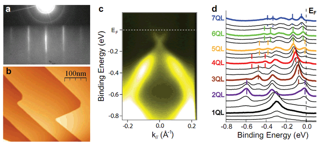 |
| FIG. 1. RHEED pattern (a), STM image (b), and ARPES spectra (c) of a MBE-grown Bi2Se3film. (d) Thickness-dependent normal photoemission spectra of Bi2Se3film indicating layer-by-layer growth of Bi2Se3film. |
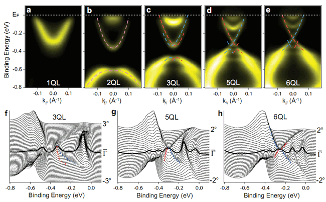 |
| FIG. 2. Thickness-dependent evolution of the ARPES band maps (a)-(e) and corresponding energy distribution curves (f)-(g) of Bi2Se3films. |