An Anisotropic Etching Effect in Graphene Basal Plane
Date:28-09-2010 Print
Graphene is a new form of carbon materials discovered by scientists after fullerenes and carbon nanotubes. As a two-dimensional quantum system stable at room temperature, graphene is the first material that conflicts with the previous theory of condensed matter physics, which predicted that the strict two-dimensional crystals can not exist in a limited temperature. The discovery of graphene will have a major impact on the development of Condensed Matter Physics. Moreover, graphene has shown unique electrical transport property, optical coupling property, and other novel physical properties. It can be patterned through two-dimensional lithography process, which may have potential applications in molecular electronics, micro/nano devices, ultra high-speed computer chips, high efficiency battery, solid-state gas sensors, terahertz science and other areas as well.
However, due to the zero energy gap behavior in graphene, it is difficult to achieve switching characteristics in graphene-based transistor devices. The metal property of graphene is a main challenge for its applications. How to introduce an energy gap in graphene becomes a hot issue. Usually, the methods for opening the energy gap include the following: (1) Using the symmetry breaking field or interactions to split the Landau level so as to form a energy gap between the conduction band and the valence band. This is mainly realized by introducing symmetry breaking in the bilayer graphene system through doping, applied electric field, or chemical potential, etc. (2) Employing the quantum confinement effect and edge effect, an energy gap can be formed in graphene nano-structures (such as nanoribbons). The size of the energy gap can be adjusted by the ribbon width. (3) Doping graphene through chemical vapor deposition (such as B, N, etc.) The modulation of the energy gap can be achieved by adjusting the doping level. (4) Substrate induced energy gap (such as epitaxial graphene on a SiC substrate). The energy gap can be controlled by adjusting the graphene-substrate interaction. Previously, in collaborations with the groups lead by Prof. Guangyu Zhang, Prof. Hongjun Gao and Prof. Xiaolong Chen, the team has systematically studied the substrate charge transfer mechanism in epitaxial graphene by Raman scattering spectroscopy. Their result provided a technical reference for the future production of epitaxial graphene based electronics devices. The result has been published in【J. Appl. Phys. 107, 034305, (2010)】.
Based on these experimental results, it is agreed that the most feasible and applicable method is to form graphene nano-structures. Currently, the preparation of graphene nano-structures has developed rapidly; however, if we want to achieve the large-scale integration of graphene nano-structure for device applications, how to use the existing micro-nanofabrication technologies to obtain graphene nanostructures with controlled edges and controlled widths is a critical problem needed to be resolved. So far, anisotropic etching of graphene has been realized by either catalytic nanoparticles cutting (Nano. Lett., 8, 1912 (2008), Nano. Lett., 9, 2600 (2009)) or selective reaction of oxidized graphene with SiO2 substrate (Nano. Res. 3, 110 (2010)), but it is difficult to apply such methods for a practical fabrication process as it is either substrate-limited or the cutting position, direction, and speed are not controllable.
Very recently, in collaborations with the groups lead by Prof. Guangyu Zhang of Institute of Physics, Chinese Academy of Sciences, Prof. Hongjun Gao and Prof. Enge Wang, the team has successfully realized the controllable anisotropic etching of graphene for the first time by using home-made remote inductively coupled plasma system. The etching in graphene basal plane depends strongly on their crystallographic orientation, resulting in zigzag edges formation. The etching process is attributed to hydrogenation and gasification of carbon atoms with etching dynamics consistent with methane formation. They are able to control the etching from edges by tuning the etching parameters such as plasma intensity, temperature and time duration. This dry anisotropic etching approach is ideally suitable for graphene tailoring as the etching rates can be precisely controlled and the quality of graphene can be preserved. This simple, clean, controllable and scalable technique is also compatible with existing semiconductor processing technology. Assuming that the wafer-scale single crystal graphene sample is available, this anisotropic etching technique would provide a useful tool for fabrication of large-scale graphene nanostructures, combined with the standard lithographic technique. Thus a road can be paved for future integrated graphene nanodevices, based on suitable starting materials and the advances of this anisotropic etching technique. Relevant results were published in 【Advanced Materials 22, 4014-4019, (2010)】. This work was highly evaluated by reviewers.
This work was financially supported by the Institute of Physics (IOP) start founding, the National Natural Science Foundation of China and National 973 Project of China.
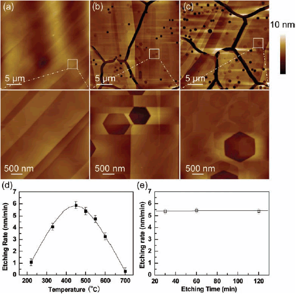 |
| FIG. 1. (a-c) AFM images of pristine and plasma etched graphite. (d) Measured maximum etching speed vs. etching temperatures. (e) Average etching speeds for graphite at different etching time intervals. |
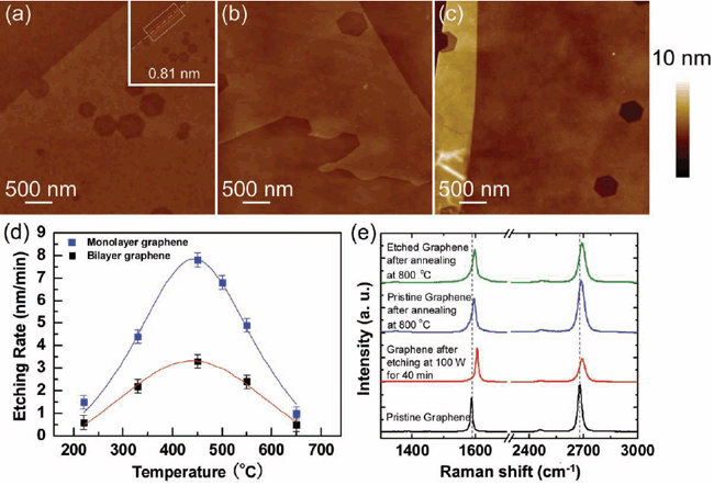 |
| FIG. 2. (a-c), AFM images of monolayer, bilayer and multilayer graphene after H2-plasma etching. (d) Measured maximum etching speed for graphene at various etching temperatures. (e) Raman spectra characterization. |
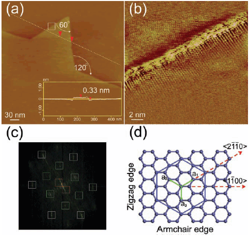 |
| FIG. 3. (a) STM image of monolayer hexagonal pits, (b) Atomic resolution image for the region marked in (a). (c) The Fourier transform (FT) spectrum of image b. (d) Schematic drawing of hexagonal graphene lattice. |
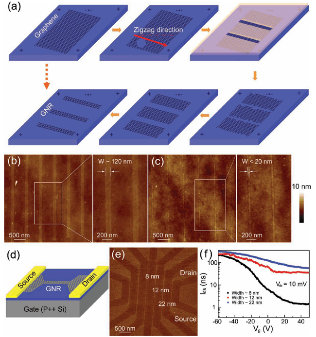 |
| FIG. 4. (a)Schematic procedures for fabricating GNR array along designed crystallographic direction by taking advantage of anisotropic etching. (b-c)AFM image for typical graphene patterns generated after O2-plasma etching and after H2-plasma etching respectively. (d)Schematic drawing of a graphene nanoribbon field effect transistor (GNR-FET). (e)AFM images of GNR-FETs with different ribbon widths. (f)Room-temperature transfer characteristics of GNR-FETs with different width. |