New and simple method for high-throughput fabrication of ultranarrow graphene nanoribbons
Date:26-04-2011 Print
The experimental discovery of graphene in 2004 has evoked ever-increasing interest in exploiting this remarkable material for future nanoelectronic applications. However, the fact that graphene is a zero-band-gap semimetal poses a major problem for its practical use in making field-effect transistors (FETs). One most important way to overcome this obstacle is to fabricate the one-dimensional (1D) ultranarrow graphene nanoribbons (GNRs) where the lateral confinement of charge carriers will open a semiconductor energy gap.
Recently, researchers in Institute of Physics, Chinese Academy of Sciences, and collaborator in Peking University, succeeded in developing an innovative approach for the high-throughput, rapid and low-cost fabrication of ultranarrow GNRs by using nanosphere lithography (NSL) nanopatterning in combination with low-power O2 plasma etching. The mystery of GNR fabrication by NSL lies in the subtle anisotropic distribution of plasma ion flux within the sphere interstices, and this approach showed the high capability and versatility for creation of the large-area, ordered GNR networks as well as a variety of interesting complex GNR architectures including chains, braches, circular rings and connected rings. By further combining NSL with photolithography patterning, the researchers have demonstrated the feasibility of controlling simultaneously both the shapes and locations of GNR architectures. Furthermore, the intrinsic simplicity of NSL nanopatterning enables this GNR-fabrication approach to be directly applicable to the pre-made graphene electrical devices, thereby achieving the straightforward “one-chip” fabrication of GNRs and band-gap tuning of graphene. It is believed that this new GNR-fabrication approach demonstrates a possible new avenue for the development of graphene-based nanoeletronics.
The research result was published in Adv. Mater. (2011, 23, 1246), and was highlighted by NPG Asia Materials entitled by “Graphene: Ribbons from spheres”.
The work has been supported by Chinese Academy of Sciences, the National Natural Science Foundation of China, and the Chinese Ministry of Science and Technology.
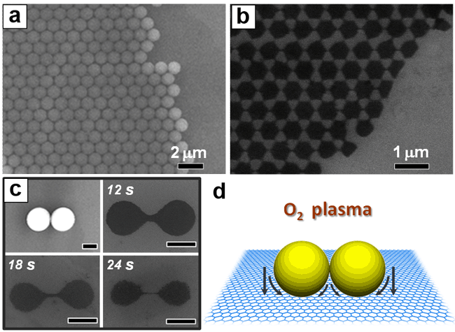 |
| Figure 1. (a) SEM image showing a domain of thehcpPS nanosphere monolayer that masking the graphene sheets. (b) SEM image of the large-area interconnected 2D GNR network etched through an hcp monolayer NSL mask. (c) SEM images showing the temporal evolution of the individual “dumbbell-like” GNRs etched through the isolated pairs of packed nanospheres (top panel. Scale bars: 500 nm. (d) Schematic illustration (not to scale) showing the NSL-defined lithographic etching process of graphene sheets. |
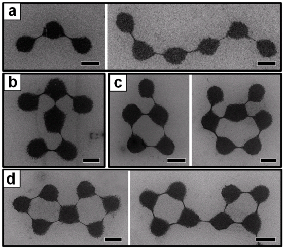 |
| Figure 2. SEM images showing some typical examples of the complex GNR architectures, including chains (a), branches (b), circular rings (c), and connected rings (d). Scale bars: 500 nm. |
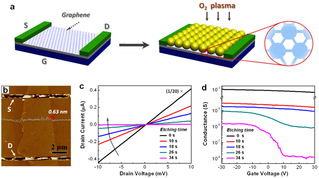 |
| Figure 3. (a) Schematic illustration of the “on-chip” band-gap tuning of graphene through NSL nanopatterning and subsequent O2-plasma etching. (b) AFM image of a typical FET device based on the mechanically cleaved single-layer graphene sheet. (c) and (d) Evolution of the device current-voltage (Id-Vds) characteristics and gate voltage (Vg) dependent conductance with respect to etching time. |