Polarization-modulated conduction and novel resistive memory in epitaxial BFO thin films
Date:23-05-2011 Print
BiFeO3 (BFO) thin films as single-phase multiferroic material show larger electric polarization and weak ferromagnetism simultaneously at room temperature. BFO is one of the prime candidates for switching magnetism with an electric field, providing an extra degree of freedom in the design of novel functional sensors and multi-state memory devices.
Recently, Dr. Can Wang and his colleagues in Prof. Kuijuan Jin’s group, in Institute of Physics, Chinese Academy of Sciences, have grown epitaxial BFO thin films successfully by using laser molecular beam epitaxy. Polarization-modulated conduction behaviors, including switchable diode effect and ferroelectric resistive switching, have been observed in the BFO thin films. These novel properties are attributed to the polarization-induced variations of Shottky barriers.
In addition, by cooperation with Fudan University, a novel ferroelectric-resistive nonvolatile random access memory consisting of the BFO epitaxial thin films has been investigated. This device has a memory that lasts for months, a sufficiently high on current and on/off ratio to permit ordinary sense amplifiers to measure “1” or “0”, and is fully compatible with complementary metal-oxide semiconductor processing.
These results are published in Appl. Phys. Lett. 98, 192901 (2011) and Adv. Mater. 23, 1277 (2011).
This work has been supported by the National Natural Science Foundation of China, and the Chinese Ministry of Science and Technology.
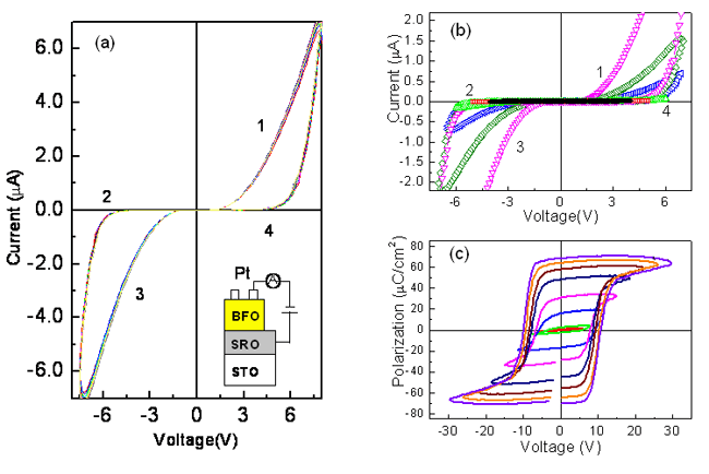 |
| Fig.1 Current-voltage curves and ferroelectric hysteresis loops. (a) IV curves of the BFO epitaxial thin films. The hysteresis of IV indicates a resistive switching behavior. (b) IV curves measured with various sweeping voltage. (c) ferroelectric polarization loops of the BFO thin films. |
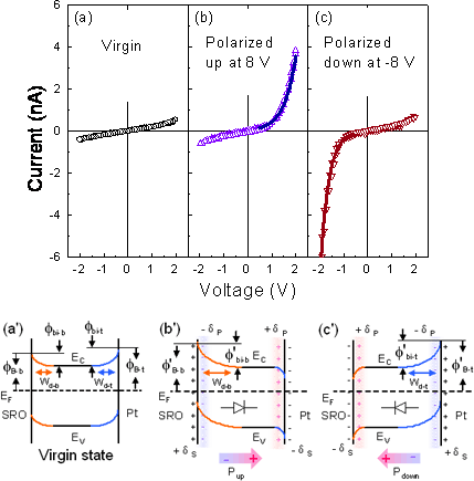 |
| Fig.2 Switchable diode effect and the possible mechanism. (a), (b) and (c) show the conduction behavior of the the BFO thin films at three different states. The thin film polarized with external field show diode-like rectifying behavior and the direction of the diode can be switched with polarization switching. (a’), (b’) and (c’) show the Schematic energy band diagrams, illustrating the variations in Schottky barriers from back-to-back diodes at virgin, to a forward diode at polarized up, and a reverse diode at polarized down, respectively. |
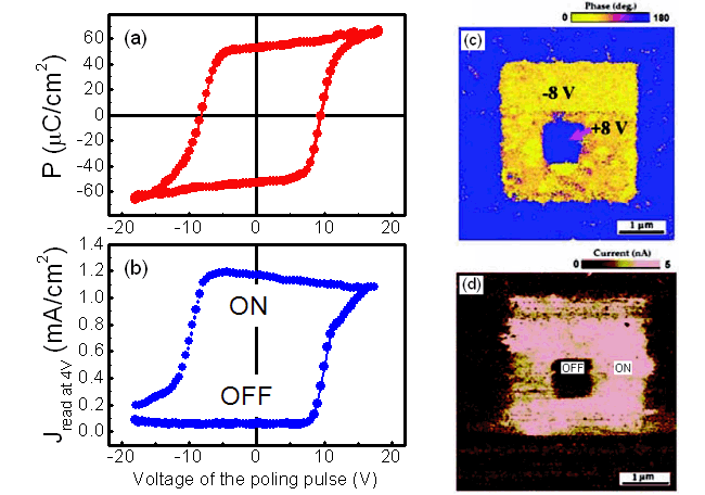 |
| Fig. 3 The evidence for polarization dependent conduction in BFO thin films. After time integrations of the displacement currents under different V, P–V hysteresis loops in (a) obtained for BFO thin films in comparison with their hysteretic current loops in (b) at fixed reading voltages of 4.0 V, after each pulse voltage in P–V loops. (c) Piezoelectric phase image of original preferred polarization patterns (downward) switched upward through PFM tip scanning of the film surface at –8 V within a square area of 3 × 3 um2. After that, the polarization in the center 1 × 1 um2area is scanned downward at + 8 V. (d) The current mapping at acquired in the same region as in (c). |