The growth, electrical tuning, and transport studies of topological insulator thin films
Date:19-08-2011 Print
Three-dimensional topological insulators are a new class of quantum materials which may host novel quantum effects such as Majorana fermions and quantized anomalous Hall effect. Harnessing the surface states could be the basis for the next generation of quantum computation and spin-based electronic devices. Recently a team of two research groups led by Prof. Kehui Wu and Prof. Yongqing Li in the Institute of Physics (IOP), Chinese Academy of Sciences and Beijing National Laboratory for condensed Matter Physics reported a series of advances in the growth of topological insulator thin films for electrical tuning and developing a new method for identifying the surface state transport.
Based on their knowledge learned from the growth of topological insulator thin films on silicon with molecular beam epitaxy [Appl. Phys. Lett. 95, 053114 (2009), Adv. Func. Mater. 21,2351 (2011).], they obtained high-quality Bi2Se3 thin films on SrTiO3, an excellent substrate material with very high electric breakdown threshold (Fig. 1). Such structures allow for large tunability in the carrier densities with back-gates. When a sufficiently large negative gate voltage is applied, the bulk conductivity can be greatly suppressed as a result of lowering the chemical potential from the bulk conduction band into the band gap and even below the Dirac point (Fig. 2). They also showed that for the first time, the gate voltage could induce significant changes in magnetoconductivity due to weak antilocalization, a quantum transport phenomenon associated with Berry phase of electrons [Phys. Rev. Lett. 105, 176602 (2010)]. The weak antilocalization can in principle protect the surface state electrons against localization regardless of the strength of disorder.
The weak antilocalization, however, also exists in non-Dirac electron systems with sufficiently strong spin-orbit coupling. For instance, a gold thin film would exhibit magnetoconductivity with the same form as one surface of a topological insulator. The latest work of the IOP team showed that for topological insulator thin films with the Fermi energy located in the conduction band, the magnetotransport follows the same equation as the topologically trivial gold thin films. In contrast, by applying negative gate voltage, they could create two separated conducting channels on the top and bottom surfaces and obtain clear deviation of the magnetotransport from the topologically trivial form. Their work thus establishes using weak antilocalization as a convenient method for detecting the surface transport, which is a key starting point for exploring various topological effects and device applications [Phys. Rev. B 83, 241304(R), Editors’ Suggestions].
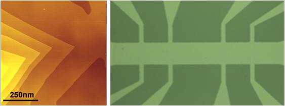 |
| Figure 1: (left) A typical STM image of Bi2Se3thin films grown on SrTO3(111) surface by molecular beam epitaxy(MBE) showing the atomically flat morphology of the film. (right) A photograph of the typical Hall device prepared for transport studies(Image by K.H. Wu et al.) |
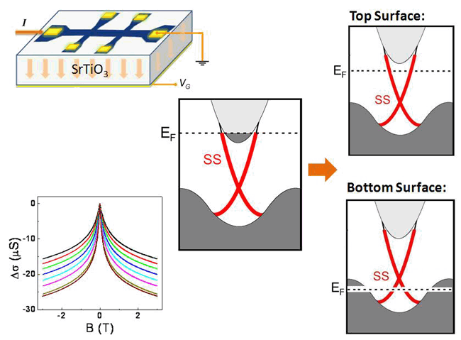 |
| Figure 2. The upper left shows a schematic drawing of the Hall device with backgate, made on Bi2Se3films grown on SrTiO3. The lower left shows the measured magnetoconductivy at different gate voltage. The three images in the right side illustrate the effect of gate tuning: The Fermi energy at the top surface and bottom surface can be tuned to different sides of the Dirac point, resulting in a dual channel system with coexisting electron and hole carriers. (Image by K.H. Wu et al.) |