Ferroelectric Gated Electrical Transport in CdS Nanotetrapods
Date:22-08-2011 Print
Complex nanostructures such as multi-armed II-VI semiconductor nanotetrapods, which normally consist of four wurtzite-structured “arms” projecting out at the tetrahedral angle bridged at a pyramidal shaped zincblende-structured “core”, are promising building blocks for next-generation nanoelectronics. As revealed theoretically, the band offset at the zincblend/wurtzite interface can result in an electron localization in the zincblende core and a hole localization in the wurtzite arms, which is expected to have significant implications in the electrical transport properties of semiconductor nanotetrapods.
Recently, researchers in Institute of Physics, Chinese Academy of Sciences, in collaboration with Peking University and Oak Ridge National Laboratory of USA, succeeded in fabrication of cadium sulfide (CdS) tetrapod-based field-effect transistors (FETs) with ferroelectric Ba0.7Sr0.3TiO3 (BST) film as high-к, switchable gate dielectrics. A cryogenic four-probe scanning tunneling microscopy is used to probe the electrical transport through individual nanotetrapods, which reveals a p-type field effect up to room temperature. The conductance modulation in the FET originates from the channel tuning in the arm-core-arm junctions of nanotetrapods. At low temperature (8.5 K), the nanotetrapod devices exhibit a single-electron transistor (SET) behavior, with a well-defined nonvolatile memory effect enabled by the reversible remnant polarization of the ferroelectric gate dielectric.
The research result has recently been published in Nano Letters 11,1913 (2011).
The work has been supported by Chinese Academy of Sciences, the National Natural Science Foundation of China, and the Chinese Ministry of Science and Technology.
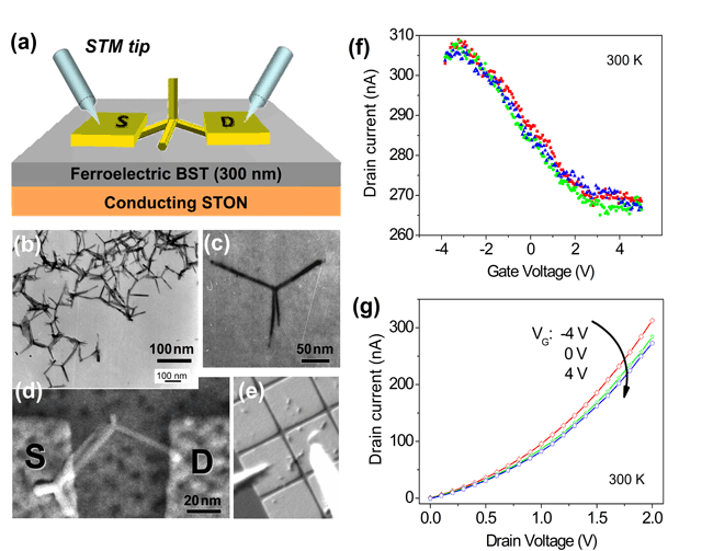 |
| Figure 1. (a) Schematic illustration of a tetrapod transistor under testing with STM tips. (b) Representative TEM image of the multi-armed CdS nanorods used in this study. The enlarged micrograph of an individual CdS tetrapod is shown in (c). (d) SEM image of a single CdS tetrapod device. The tetrapod here has a fractured arm. (e) in-situ SEM image of two STM tips (in white) probing on a testing device. (f) Typical transfer characteristics of single CdS nanotetrapod device. (g) The current versus source-drain bias voltage curves of the nanotetrapod under gate voltages of -4 V, 0 V, and 4 V. |
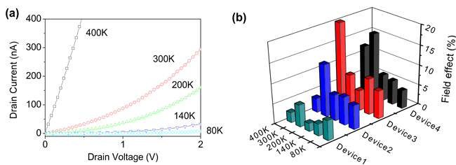 |
| Figure 2. Temperature dependant electrical characteristics of the nanotetrapod device. (a) Typical temperature dependent I-V curves of the nanotetrapod with VG=0 V, measured at 80 K, 140 K, 200 K, 300 K, and 400 K, respectively. (b) The magnitudes of the field effect ((Imax-Imin)/Imax× 100 % at ±4 V) of four different nanotetrapod transistors measured at different temperatures. |
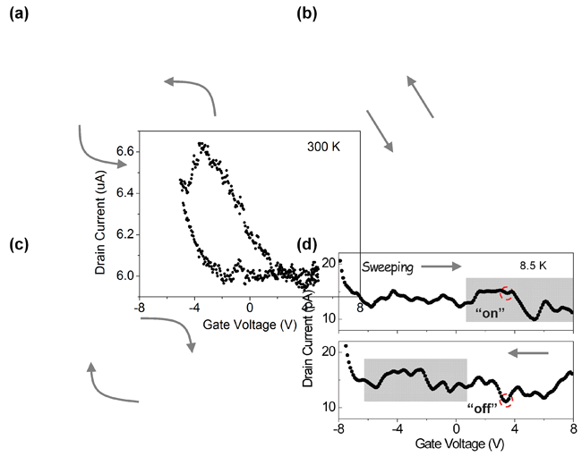 |
| Figure 3. Typical I-VGtransfer characteristic measured at 300 K (a), 140 K (b), 80 K (c), and 8.5 K (d), respectively (with VSD=2 V for a, b, and c; VSD=50 mV for d). A counter-clockwise hysteresis loop occurs at room temperature (a) due to a charge-storage effect; while a competition between the ferroelectric effect and the charge-storage effect essentially closes the memory window at 140 K (b). At 80 K (c), a clockwise hysteresis loop is opened, indicative of a nonvolatile memory operation. At 8.5 K (d), a ferroelectric-modulated SET behavior is observed. The two red circles represent a bi-stable state. The sharp increase at a gate voltage of -6 V is due to leakage current. |