Zigzag-edged Graphene Nanostructures for future graphene electronics
Date:01-09-2011 Print
Graphene, a monolayer of covalently bonded carbon atoms, due to its extraordinarily high carrier mobility and excellent chemical stability, is considered to be a potential material for future electronics. Edge displays a crucial role in graphene nanostructure’s electrical properties. For example, graphene nanoribbon with zigzag edge behaves like metal, while graphene nanoribbon with armchair edge exhibit semiconducting property. As graphene nanostructures with specific edges are basic blocks of graphene electronics, how to effectively fabricate them appear to be crucial and urgent.
Various approaches, such as chemical exfoliation of graphite, unzipping of carbon nanotubes, lithographic and nanowire-template etching of graphene, and covalent assembly of molecular building blocks, have been developed for graphene nanostructure fabrication, but zigzag edges in those graphene structures have not been achieved yet.
Guangyu Zhang, a professor of physics at Institute of Physics of CAS, and his research group observed an anisotropic etching effect in graphene basal plane in 2010 [Advanced Materials 22, 4014, (2010)]. Recently, they creatively combine this effect with standard microfabrication and developed a well-controlled top-down approach to fabricate zigzag-edged graphene nanostructures. This approach consists of two key steps: artificial defects patterning and H-plasma etching. With this approach, they achieved various graphene nanostructures with zigzag edges, such as sub-10-nm wide zigzag-edge graphene nanoribbons (Z-GNRs), graphene superlattice, triangular graphene islands, etc. For the as-fabricated Z-GNRs, they confirmed the metallic edge states from the electrical transport measurements. Furthermore, they found a reduced edge scattering effect for charge carriers and a characteristic phonon mode in Z-GNRs. These results were published in Advanced Materials 22, 3061-3065 (2011).
This approach opens a gateway to experimentally studying the rich properties of zigzag edged graphene nanostructures. Besides, the clean graphene patterning technique, which is compatible with the established semiconductor technology, shows great promise for making future graphene devices or circuits.
This work was supported by NSFC and National 973 projects.
Paper URL:
1、“Patterning Graphene with Zigzag Edges via Self-Aligned Anisotropic Etching”
http://onlinelibrary.wiley.com/doi/10.1002/adma.201100633/pdf
2、“An Anisotropic Etching Effect in the Graphene Basal Plane”
http://onlinelibrary.wiley.com/doi/10.1002/adma.201000618/pdf
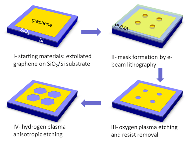 |
| Figure 1. Schematic of the fabrication process. (I), Mechanically exfoliated bilayer or multilayer graphene used as starting materials. (II), PMMA resist mask formed by e-beam lithography. (III), O-plasma etching for artificial defects formation. ( IV), Anisotropic etching by H-plasma, resulting in hexagonal holes growth from original circular holes. (Image by Guangyu Zhang et al.) |
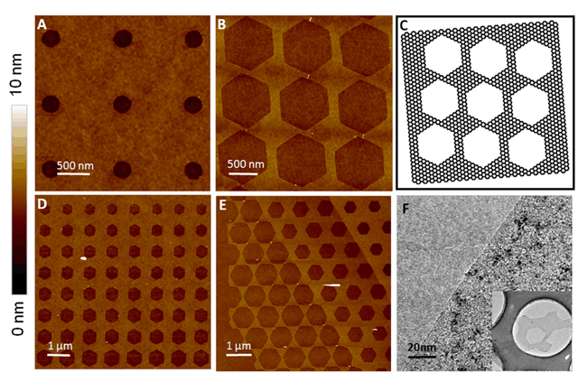 |
| Figure 2. Patterns before and after anisotropic etching. (A), AFM image of graphene patterned with an array of circular holes fabricated by e-beam lithography and O-plasma etching. During H-plasma etching, all circular holes grow and take hexagonal shapes, as shown in (B). (C), illustration of atomic structure of the H-plasma etched graphene in (B), showing all etched edges are zigzag-type. (D), Hexagonal pits grown in bilayer graphene from different-sized original holes after H-plasma etching. (E), Hexagonal pits grown in bi-, tri- and multi- layer graphene from same-sized original holes after H-plasma etching. (F), TEM image of an etched hexagon (inset) edge shows edge roughness less than 1 nm. The black contaminations are PMMA residues adsorbed during sample transfer procedure from SiO2/Si substrate to TEM grid. (Image by Guangyu Zhang et al.) |
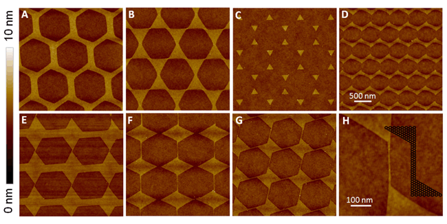 |
| Figure 3. Various patterned graphene nanostructures. (A) and (B), honeycomb-like networks. (C), array of isolated triangular dots with sizes around 200 nm. (D), waved ribbons array. For (A), (B), (C) and (D), the original designed pattern was hexagonal close-packed circular holes array while for (E), (F) and (G), square-arranged circular holes array was applied. The different patterns in (A), (B) and (C) are generated due to the differently designed patterns along different crystallographic orientation in the graphene and different etching times. (E), (F) and G are aligned GNRs with different lengths. (H), a zigzag-edge GNR with a width of ~5nm. In all patterns, except (D) and (H), the pitch distances for neighbouring hexagons are 1 μm. (Image by Guangyu Zhang et al.) |
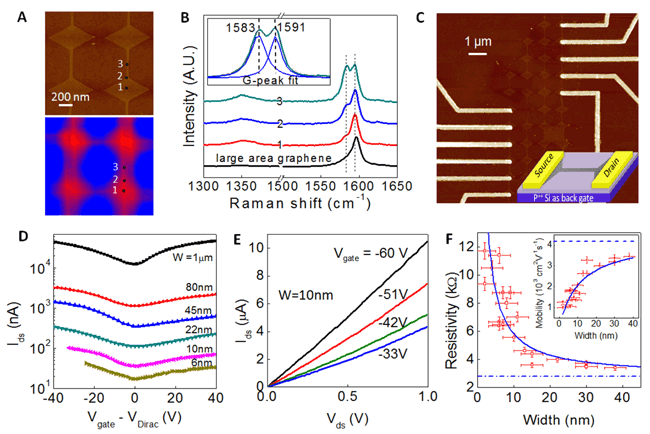 |
| Figure 4. Raman and electrical characteristics of Z-GNRs. (A), (top) AFM image of patterned graphene consisting of Z-GNRs and graphene pads, and (bottom) the corresponding Raman G-peak intensity mapping image. (B), Raman spectrum of patterned graphene at the three positions marked in (A) and of large-area graphene for comparison. (C), AFM image of devices made of ~10nm-wide Z-GNRs, and the inset is a schematic drawing of the device structure. (D), transfer characteristics (current versus gate voltage) for Z-GNR devices with different widths. The channel length for these devices is around 500 nm. Source-drain bias is 10mV. (E), output characteristics recorded under various Vgs for a typical ~10nm-wide zigzag ribbon device. (F), maximum resistivity at charge neutral point of Z-GNRs plotted against ribbon width. Inset of (F), carrier mobility plotted against ribbon widths. The dashed lines in (F) and inset are the resistivity and carrier mobility for pristine graphene. |