Bandgap Engineering of MgZnO Materials and High Performance Solar-blind UV Detectors
Date:05-09-2011 Print
Solar-blind materials based on wide bandgap semiconductors such as AlGaN, diamond and MgZnO, have received tremendous attention due to their potential applications in solar-blind ultraviolet (UV) detection. MgZnO is one of the most competitive candidates for its tunable bandgap hopefully covering the whole solar-blind spectrum region (220~280 nm), as well as its large exciton binding energy, and more importantly, much lower growth temperature than AlGaN etc. Recently a team consisting of three research groups led by Prof. DU Xiaolong, Prof. YU Richeng, and Prof. GU Changzhi in the Institute of Physics, Chinese Academy of Sciences (IOP) and Beijing National Laboratory for Condensed Matter Physics reported a series of advances in the epitaxial growth of high-Mg-content MgZnO thin films as well as fabrication of solar-blind UV photodetectors with high performance.
They firstly determined the important role of low deposition temperature and oxygen-rich conditions in suppressing the well-known phase segregation problem during the growth of high-Mg-content MgZnO epitaxial films by molecular beam epitaxy. A unique in-situ metal-flux monitoring technique was also developed to realize the precise control of reactive metal (Mg for instance) flux in oxygen environment, which guarantees the experimental results repeatable and reliable. A low-Mg-content “quasi-homo” buffer layer was further creatively adopted to accommodate the big discrepancy in crystal structures and atomic bonding configurations between high-Mg-content MgZnO epilayer and substrates. As a consequence, single-phase wurtzite Mg0.55Zn0.45O components were achieved on ?-Al2O3 substrate with a solar-blind band gap of 4.55 eV (272 nm), which is the highest value ever reported [Adv. Mater., 21, 4625 (2009)]. Prototype solar-blind UV detectors were fabricated on the high quality films, and the device shows a sharp deep-UV cutoff at 270 nm, a fast response – less than 500 ns – and a high rejection ratio of solar-blind UV to visible light of more than two orders of magnitude [Appl. Phys. Lett. 98, 103506 (2011)]. (Fig. 1)
For potential integration of MgZnO optoelectronic device with the well-developed Si microelectronic technologies, n-MgZnO/p-Si heterojunction solar-blind UV detector is also highly desirable. However, the epitaxial growth of high-quality MgZnO films on Si substrate is a challenge due to the formation of amorphous SiOX layer at the initial growth stage of oxides. Another challenge is the creation of a suitable epitaxial template for high-Mg-content MgZnO. An interfacial layer with 4-coordinated bonding configuration is essential to avoid the occurrence of phase separation. In this case, the low-temperature interface engineering technique they introduced in high quality ZnO epitaxy on Si [Appl. Phys. Lett. 90, 151912 (2007)] cannot be used in this heterostructure. According to these necessities, Be and BeO were applied to replace Mg and MgO, repectively, in fabrication of solar-blind wurtzite MgZnO film on Si. It is found that Be/Si interface is more stable than Mg/Si interface, and BeO is more favorable to increase Mg content in MgZnO film, which has been confirmed by the accomplishment of single crystalline Mg0.44Zn0.56O film with a solar-blind band gap of 4.43 eV (280 nm). The interface controlling significantly improves the device performance, as the photodetector demonstrates a sharp cutoff wavelength at 280 nm with a higher photoresponsivity of 0.04 A/W [Appl. Phys. Lett. 98, 221902 (2011)]. A comparative study of n-Mg0.4Zn0.6O/p-Si UV-B photodetector was further carried out to investigate the influence of device structure on device performance. The role of built-in field and low interface scattering in p-n heterojunction is explored, and the energy band diagram of n-MgZnO/p-Si is employed to interpret the efficient suppression of visible light photoresponse from Si substrate [Appl. Phys. Lett. 98, 263501 (2011)]. (Fig. 2) A series of patents have been applied or authorized in these studies (patent numbers:201110119774.2, 201110156368.3, 201110010442.0, 201010191983.3, 201010219623.X, 200810224529.6, ZL200810104269.9).
The work has received support from the National Natural Science Foundation of China, the Ministry of Science and Technology of China, and Chinese Academy of Sciences.
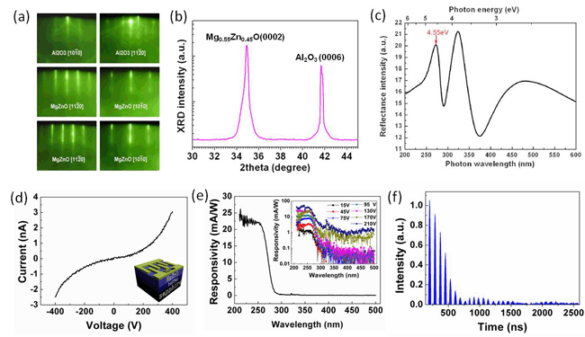 |
| Fig. 1. (a) RHEED evolutions inW-Mg0.55Zn0.45O growth on sapphire;(b) XRD θ-2θ scan result of W-Mg0.55Zn0.45O single crystalline film; (c) Reflectance spectrum of W-Mg0.55Zn0.45O film measured at room temperature and the red arrow indicates the band gap position; (d) Dark current-voltage (I-V) characteristic of the Mg0.55Zn0.45O solar-blind UV detector (the inset is a schematic of the detector structure); (e) Spectral photoresponse of the Mg0.55Zn0.45O solar-blind UV detector at 130V bias (the inset is photoresponse spectra at different biases); (f) Temporal response of the Mg0.55Zn0.45O solar-blind UV detector. (Image by Xiaolong Du et al.) |
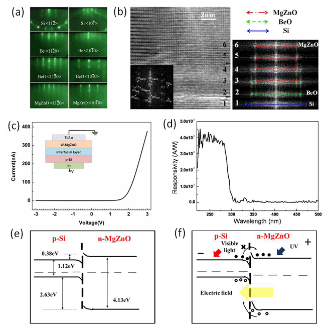 |
| Fig. 2. (a) RHEED evolutions in W-MgZnO growth on Si (111)-1×1 surface; (b) Cross-sectional HRTEM micrograph along <11-2>Sidirection near the interface region and the corresponding FFT patterns; (c) Current-voltage (I-V) characteristic of the n-MgZnO (0001)/p-Si (111) heterojuntion photodetector. The inset provides the detailed device structure; (d) Photoresponse spectrum of the photodetector at 0.5 V bias; (e) Energy-band diagram of n-MgZnO/p-Si heterojunction under equilibrium condition; (f) Energy-band diagram of n-MgZnO/p-Si heterojunction under illumination at 3 V reverse bias. (Image by Xiaolong Du et al.) |