Scientists discover a new technique for patterning of graphene nanostructures
Date:16-10-2012 Print
Graphene has recently attracted intensive interests for its unique physical properties. Graphene nanostructures are proposed as the building block for graphene electronics. The controllable fabrication of nanostructures is indispensable for graphene photoelectronics, spintronics, mechanical and biological sensors. Two major strategies have been developed so far to fabricate graphene nanostructures: bottom-up synthesis and top-down cutting of graphene. Top-down cutting of graphene is a controllable, scalable, and semiconductor-technology-compatible approach for patterning of graphene nanostructures. Recently, various top-down cutting approaches have been developed; however, it remains a challenge for facile fabricate of graphene nanostructures in an easy and controllable manner.
The research groups led by Prof. ZHANG Guangyu in the Institute of Physics (IOP), Chinese Academy of Sciences, and Beijing National Laboratory for Condensed Matter Physics is recently focusing on graphene nanostructure fabrications and the related electrical transport studies. Previously, they have reported a highly anisotropic dry-etching technique in graphene basal plane for the first time [Advanced Materials 22, 4014, (2010)]; they have also creatively combined this technique with artificial-defects engineering for well-controlled top-down cutting of graphene nanostructures with zigzag-edges and sub-10-nm feature sizes [Advanced Materials 23, 3061, (2011)]. They have also studied Raman scattering of graphene nanoribbons with Hydrogen-terminated zigzag edges and found the electron-phonon coupling in these unique structures [Nano letters 11, 4083-4088 (2011)].
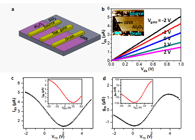
Recently, XIE Guibai, a doctoral candidate in this group, and his colleges reported a new approach for graphene nanostructures patterning, named graphene edge lithography (GEL). This new technique is easy, efficient, and controllable. Compared with standard lithographic fabrication techniques using photoresist for mask layer generation, this approach uses selective coatings on the graphene edges as a hard mask for pattern formation. Selective high-k dielectric coatings on graphene edges were performed in atomic layer deposition (ALD) system and graphene nanostructure formation was achieved by removal of uncoated graphene by dry etching. Graphene nanoribbons and nanorings have been successfully and reproducibly fabricated with relatively-high quality and well-defined widths down to ~5 nm. Besides, the ALD mask layers could be also used as the dielectric layers for top-gated devices, demonstrating another advance of this technique. Top-gated GNRs transistor devices with the carrier mobility up to 400 cm2/V·s were investigated, and a more than 10-fold increase in transconductance was observed, compared with those of the back-gated devices. This method allows easy and reproducible fabrication of various graphene nanostructures. This research result has been published in Nano Letters 12, 4642–4646 (2012).
This work was supported by NSFC, National Basic Research Programs of China.
1、“Patterning Graphene with Zigzag Edges via Self-Aligned Anisotropic Etching”
http://onlinelibrary.wiley.com/doi/10.1002/adma.201100633/pdf
2、“An Anisotropic Etching Effect in the Graphene Basal Plane”
http://onlinelibrary.wiley.com/doi/10.1002/adma.201000618/pdf
3、“Observation of Raman G-Peak Split for Graphene Nanoribbons with Hydrogen-Terminated Zigzag Edges”
http://pubs.acs.org/doi/abs/10.1021/nl201387x
4、“Graphene Edge Lithography”
http://pubs.acs.org/doi/abs/10.1021/nl301936r
 |
| Figure 1. Schematic of the graphene edge lithography. The process includes selectively ALD of Al2O3/HfO2on graphene edges, dry etching of the unprotected graphene and KOH etching of the metal oxides.(Image by ZHANG Guangyu et al ) |
 |
| Figure 2. Fabrication of graphene nanostructrues by GEL. In figure c, the width of graphene nanoribbon is ~15 nm and the neighboring distance of the parallel bilayer GNR arrays is ~30 nm. (Image by ZHANG Guangyu et al ) |
 |
| Figure 3. Room-temperature electrical transport measurements of the top-gated GNR devices fabricated from mechanically cleaved graphene edges. (Image by ZHANG Guangyu et al ) |


