A novel method discovered to control resonant tunneling to enhance field electron emission properties of unique diamond film cold cathods
Date:09-11-2012 Print
Resonant tunneling has so far been reported only for semiconductor materials. However, recently, Prof. GU Changzhi and Prof. LU Wengang at the institute of Physics (IOP), Chinese Academy of Sciences (CAS) in collaboration with Prof. JIANG Xin at Siegen University of Germany and Prof. S. Mantl at Research Center Juelich GmbH of Germany, reported a novel method to realize and control the resonant tunneling via metallic CoSi2 interlayer to enhance the field electron emission properties of unique diamond film cold cathods.
Excellent field electron emission properties of a diamond/CoSi2/Si quantum well nanostructure are observed. The novel quantum well structure consists of high quality diamond emitters grown on bulk Si substrate with a nanosized epitaxial CoSi2 conducting interlayer. The results show that the main emission properties were modified by varying the CoSi2 thickness and that stable, low-field, high emission current and controlled electron emission can be obtained by using a high quality diamond film and a thicker CoSi2 interlayer. A new electron resonant tunneling mechanism in this quantum well structure is suggested. This material meets most of the requirements for development of vacuum microelectronic devices and large-area cold cathodes for flat-panel displays.
Further, for display applications, the stable, low-threshold and high-current-density emitter made of high quality diamond on CoSi2 will likely be used in integrated circuits in combination with other semiconductor devices to realize the controlled and addressed display by selective growth of epitaxial CoSi2 films of different thicknesses in nanoscale, which can be realized accurately and easily with the current CoSi2 growth technology.
The related result is published in Scientific Reports. 2, 746(2012). This work is supported by grants from the National Natural Science Foundation of China and the Ministry of Sciences and Technology of China, and Chinese Academy of Sciences.
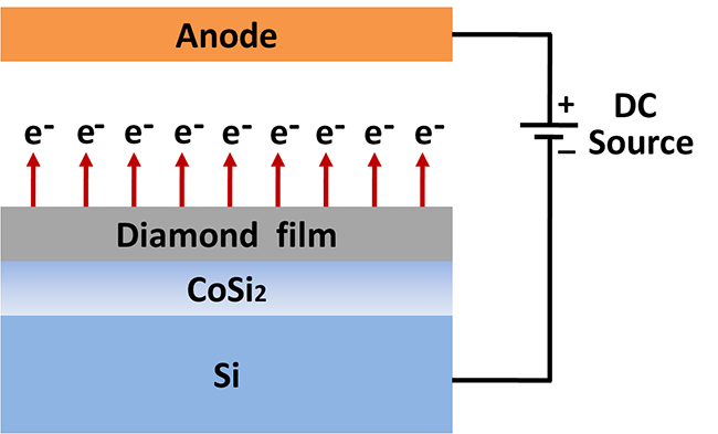 |
| Figure 1 Schematic diagram of diamond/CoSi2/Si quantum well cathode.(Image by GU Changzhi et al) |
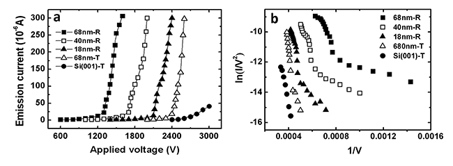 |
| Figure 2 I-V emission curves (a) and corresponding FN plots (b) obtained from diamond films deposited on (001) CoSi2having different thicknesses and on (001) Si. 68 nm-R, 40 nm-R and 18 nm-R represent the randomly oriented diamond films grown on 68 nm, 40 nm and 18 nm thick CoSi2. 68 nm-T represents (001)-textured diamond film grown on 68 nm thick CoSi2. (001) Si-T represents (001) epitaxial diamond film grown on (001) Si. (Image by GU Changzhi et al) |
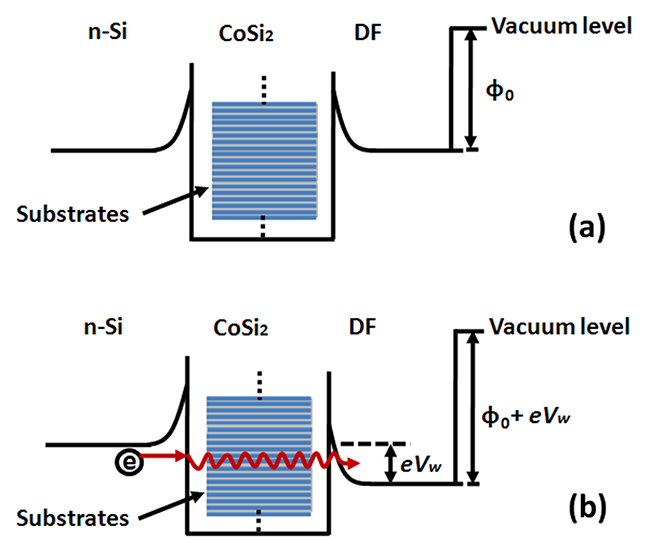 |
| Figure 3 Schematic band edge diagram of the n-Si/ CoSi2/DF double barrier structure under (a) zero bias and (b) finite bias. An electron with an energy within the energy window indicated as eVwtunnels the Schottky barrier from n-Si to CoSi2film, resonant between the double barriers and tunnel the other Schottky barrier from CoSi2to DF. Work function of the DF surface are adjusted by eVw. (Image by GU Changzhi et al) |