Highly Tunable Propagating Surface Plasmons on Supported Silver Nanowires
Date:15-04-2013 Print
The manipulation of light at the nanometer scale is important for both fundamental researches and actual applications. Surface plasmons (SPs) on metal nanostructures provide the possibility for manipulating light at the nanometer scale. For instance, due to the strong field confinement effect in metal nanowires (NWs), these 1-D structures can overcome the diffraction limit imposed on conventional optical components to support SP propagation within sub-wavelength volume, which serves as the basis for high density packing of optical circuits
In recent years, Prof. XU Hongxing and his research team in Institute of Physics, Chinese Academy of Sciences, have conducted a series of original research work aiming at the fundamental properties of metal nanowire-based integrated nano-optical circuits, including interactions between NW SPs and single molecules or quantum dots, angular emission of NW SPs, correlation between incident and emitted light polarizations, influences of substrate and NW curvature on the SP propagation, chiral SP propagation, and routing effect in branched NW structures.
In 2011, they reported the realization of a complete family of binary logic functions, and further demonstrated that a plasmonic NOR gate, a ‘universal logic gate’, can be realized through cascaded OR and NOT gates in four-terminal plasmonic nanowire networks (Nano Lett. 2011, 11, 471; Nature Communications 2011, 2, 387).
The development of SP-based nanophotonic devices relies on the precise control of the near field and propagation of SPs. Recently, they discovered an extremely large tunability of propagating SPs on substrate-supported Ag NWs using the quantum dot fluorescence imaging technique. By changing the thickness of the coated Al2O3 layer on the NW, they systematically investigated the period change of the near field pattern. Their results show that the period is sensitive to the coating thickness. By applying a 1 nm thick dielectric coating layer of Al2O3, the period is increased by about 90 nm. For bulk changes in the surrounding medium, a period increase of about 16 μm per refractive index unit was observed. This high sensitivity effect is explained by considering the propagation constants and the dispersion curves of NW SPs. They demonstrated that such giant modulation of SPs can be used to design functional plasmonic circuits. In a Ag NW network, the output signal can be largely changed by adding additional 5 nm of Al2O3. This discovery of large tunability of the propagating SPs on Ag NW networks thus provides a simple and robust way for the exact control of SP near-field distributions and the precise routing of optical signals in circuitries. In addition, the highly tunable near field distribution on supported Ag NWs can also be used for new types of ultrasensitive on-chip optical sensors.
This work was published on Proceedings of the National Academy of Sciences of USA [PNAS 2013, 110, 4494-4499]. It was supported by Chinese Academy of Sciences, National Natural Science Foundation of China, and The Ministry of Science and Technology of China.
CONTACT:
Prof. XU Hongxing
Institute of Physics, Chinese Academy of Sciences
Email: hxxu@iphy.ac.cn
In recent years, Prof. XU Hongxing and his research team in Institute of Physics, Chinese Academy of Sciences, have conducted a series of original research work aiming at the fundamental properties of metal nanowire-based integrated nano-optical circuits, including interactions between NW SPs and single molecules or quantum dots, angular emission of NW SPs, correlation between incident and emitted light polarizations, influences of substrate and NW curvature on the SP propagation, chiral SP propagation, and routing effect in branched NW structures.
In 2011, they reported the realization of a complete family of binary logic functions, and further demonstrated that a plasmonic NOR gate, a ‘universal logic gate’, can be realized through cascaded OR and NOT gates in four-terminal plasmonic nanowire networks (Nano Lett. 2011, 11, 471; Nature Communications 2011, 2, 387).
The development of SP-based nanophotonic devices relies on the precise control of the near field and propagation of SPs. Recently, they discovered an extremely large tunability of propagating SPs on substrate-supported Ag NWs using the quantum dot fluorescence imaging technique. By changing the thickness of the coated Al2O3 layer on the NW, they systematically investigated the period change of the near field pattern. Their results show that the period is sensitive to the coating thickness. By applying a 1 nm thick dielectric coating layer of Al2O3, the period is increased by about 90 nm. For bulk changes in the surrounding medium, a period increase of about 16 μm per refractive index unit was observed. This high sensitivity effect is explained by considering the propagation constants and the dispersion curves of NW SPs. They demonstrated that such giant modulation of SPs can be used to design functional plasmonic circuits. In a Ag NW network, the output signal can be largely changed by adding additional 5 nm of Al2O3. This discovery of large tunability of the propagating SPs on Ag NW networks thus provides a simple and robust way for the exact control of SP near-field distributions and the precise routing of optical signals in circuitries. In addition, the highly tunable near field distribution on supported Ag NWs can also be used for new types of ultrasensitive on-chip optical sensors.
This work was published on Proceedings of the National Academy of Sciences of USA [PNAS 2013, 110, 4494-4499]. It was supported by Chinese Academy of Sciences, National Natural Science Foundation of China, and The Ministry of Science and Technology of China.
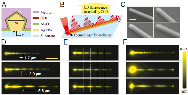 |
| (A) Schematic cross-section of the samples. (B) Schematic illustration of the excitation/collection configuration and the SPs propagating along the NW. (C) SEM images of NWs coated with Al2O3layers of different thickness. (D-F) Near-field distribution images for NWs with different dielectric environments. . (Image by Prof. XU Hongxing et al.) |
CONTACT:
Prof. XU Hongxing
Institute of Physics, Chinese Academy of Sciences
Email: hxxu@iphy.ac.cn