A breakthrough in graphene epitaxy and 2D superlattice
Date:17-09-2013 Print
Graphene has attracted broad interests in the field of condensed mater physics and materials science owning to its superior electronic, optical and mechanical properties. It is known that commonly used SiO2 substrates would severely degrade the quality of graphene via extra charge carrier scattering and electron-phonon interaction. Thanks to the atomic smooth surface, absence of dangle bonds, and minimum charge doping, hexagonal boron nitride (h-BN) was recently found an extraordinary substrate on which graphene’s intrinsic properties could be largely preserved. More importantly, a 2D superlattice could be created in graphene on h-BN (G/h-BN) due to their lattice mismatch. Theory predicted that this superlattice would reshape the band structure of graphene, causing additional superlattice Dirac point. Such graphene 2D superlattice is a novel platform for addressing new physics such as Hofstadter Butterfly spectrum.
In order to put graphene on h-BN, a so-called “transfer” technique has been developed; however, such technique brings fabrication complexity and structure uncertainty. For example, graphene stacking on h-BN is random and hard to control; as a result, as-made graphene superlattice differs from one another. This transfer technique also suffers from structural inhomogeneities and interface contaminations. In this aspect, control of stacking order of G/h-BN, so as to obtain well-defined and uniform 2D superlattice in a large scale, meanwhile maintaining the high quality without contaminations, is very challenging.
Now, a research group led by Prof. ZHANG Guangyu in the Institute of Physics, Chinese Academy of Sciences, in collaboration with Prof. ZHANG Yuanbo in Fudan University and Prof. YAO Yugui in Beijing Institute of Technology, have made a breakthrough on control of graphene stacking order on h-BN. Based on their previously developed graphene growth techniques [refer to: Nano Res. 2011, 4, 315; Small 2012, 8, 1429; Nano Res. 2012, 5, 258], they realized, for the first time, Van de Waals epitaxy of graphene on inert substrate h-BN. The epitaxial graphene is single-crystalline, of high quality with mobilities up to 20,000 cm2V-1s-1, and has lattice orientation exactly the same with the underneath h-BN, i.e., zero lattice rotation angle. Besides, the size of epitaxial graphene can be scaled-up since it is only limited by the size of h-BN.
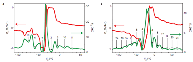
As a result of the zero lattice rotation and lattice mismatch (1.7%) between graphene and h-BN, a trigonal moiré pattern with a period of ~15nm was observed under atomic force microscope. Such moiré pattern in graphene is a 2D superlattice allowing us to reconstruct the band structure of graphene. Extra Dirac points originated from superlattice modulation were observed from electrical transport measurements. Besides the graphene intrinsic Dirac point, two satellite resistance peaks appearing at both the electron and hole branch correspond to superlattice Dirac point. In order to further study these epitaxial graphene, quantum Hall effects (QHE) measurements for both monolayer (MLG) and bilayer (BLG) graphene were carried out, yielding the observation of half integer QHE in MLG and 8-fold degeneracy at zeroth Landau level (LL) in BLG. More over, their detailed studies of MLG give LL features of the 2D superlattice, with the appearance of additional sets of peaks and valleys in the fan diagram of longitudinal Hall resistance.
This pioneer study shed some light on graphene epitaxy on many other single-crystalline substrates for creation of various well-defined 2D superlattices for band structure engineering. These research results have been published in Nature Materials 2013, 12, 792, and the project is supported by the National Science Foundation, the Ministry of Science and Technology of China, and the Chinese Academy of Science.
Contact:
Prof. ZHANG Guangyu
Institute of Physics
Chinese Academy of Sciences
Email: gyzhang@iphy.ac.cn
Tel: 82649021
Paper links:http://www.nature.com/nmat/journal/v12/n9/full/nmat3695.html
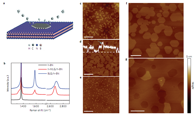 |
| Figure 1. Graphene epitaxy on h-BN with growth schematic diagram, AFM, and Raman characterization. (Image by Prof. ZHANG Guangyu et al.) |
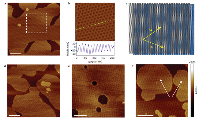 |
| Figure 2. Graphene superlattice structure characterized by AFM for various samples. (Image by Prof. ZHANG Guangyu et al.) |
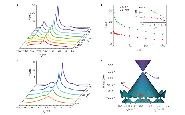 |
| Figure 3. Electrical transfer measurements and band structure of graphene superlattice. (Image by Prof. ZHANG Guangyu et al.) |
 |
| Figure 4. Quantum Hall effects (QHE) of monolayer graphene (MLG) and bilayer graphene (BLG). (Image by Prof. ZHANG Guangyu et al.) |
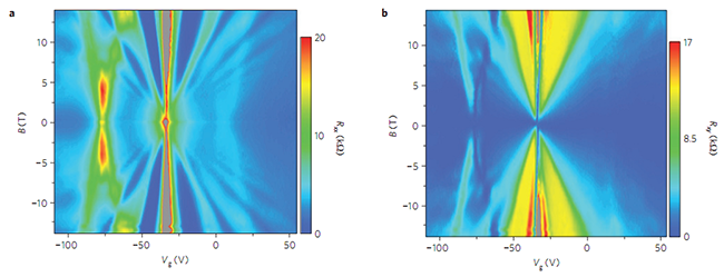 |
| Figure 5. QHE fan diagram of MLG superlattice. (Image by Prof. ZHANG Guangyu et al.) |