Commensurate–incommensurate transition in graphene on hexagonal boron nitride
Date:18-07-2014 Print
Graphene has attracted broad interests in the field of condensed mater physics and materials science owning to its superior electronic, optical and mechanical properties. Hexagonal boron nitride (hBN) was recently found an extraordinary substrate on which graphene’s intrinsic properties could be largely preserved, due to its atomic smooth surface, absence of dangle bonds, energy band gap, and minimum charge doping. Such two-dimensional (2D) hetrostructures of graphene/hBN atomic crystals provides a novel platform for addressing novel physics.
The mismatch (1.8%) between the lattice constants of hBN and graphene lead to a hexagonal moiré pattern, which has been observed by scanning probe microscopy. The periods of the moiré pattern can be modulated by the relative rotation angle (φ) between the graphene and hBN crystalline lattices. The moiré potential acts on charge carriers in graphene, resulting in a modification of its electronic spectrum, such as additional superlattice Dirac point, Hofstadter Butterfly spectrum et al. So far it has been assumed that no structural changes occur in graphene after it is brought in contact with hBN. Besides, scientists have always been puzzled by the widely different measuring properties on the graphene/hBN hetrostructures obtained from various research groups.
Recently, the group led by Prof. Hong-Jun Gao from Nanoscale Physics and Devices Laboratory, Institute of Physics, CAS, in collaboration with the Nobel laureates, Prof. A. Geim and Prof. K. Novoselov’s group from University of Manchester, UK, investigated the strain distribution in graphene on hBN for different misorientation angles (φ) between the two crystalline structures. They made a successful process of transferring precisely an exfoliated monolayer graphene onto hBN substartes, and validated a commensurate-incommensurate transition by using atomic force microscopy (AFM), scanning tunneling microscopy (STM) and Raman spectroscopy. When φ is less than 1° (large moiré periodicity, L > 10 nm), graphene stretches locally to achieve an energetically favourable state for van der Waals interactions with hBN, which results in relatively large areas of commensurate stacking and deformations concentrated in narrow strained regions. For φ > 1° (small moiré periodicity), graphene and hBN lattices remain unsynchronized and there are no distinct regions with accumulated strain (the incommensurate state). The different distributions of Young’s modulus of Graphene/hBN with various misorientation angles were first discovered from the AFM results. In order to observe directly the slight changes of lattice constants of graphene at different moiré regions, Ruisong Ma, Jianchen Lu and Dr. Haiming Guo in Gao’s group achieved the large-area, high-resolution STM images at the atomic level on the Graphene/hBN surfaces, and found 2.0 ± 0.6 % variations of C-C atomic separations in graphene among different moiré regions. This slight change in atomic separations in graphene provides a clear and direct evidence of commensurate–incommensurate transition in graphene on hBN. The differences in their structures and properties were further validated from Raman spectra and electronic transport measurements.
The discovery and investigation of such commensurate–incommensurate transition is of importance for us to understand the novel phenomena and resolve the puzzles in graphene/hBN hetrostructures. For example, a band gap can be easily found around the Dirac point for the φ < 1° (L > 10 nm) sample, while it becomes much difficult for the φ > 1° (L < 10 nm) sample. This work is a great breakthrough in the related fields in condensed-matter physics, and the main results were published on Nature Physics [10, 451–456 (2014)]. The project is supported by the National Science Foundation, the Ministry of Science and Technology of China, and the Chinese Academy of Science.
Paper link:http://www.nature.com/nphys/journal/v10/n6/full/nphys2954.html
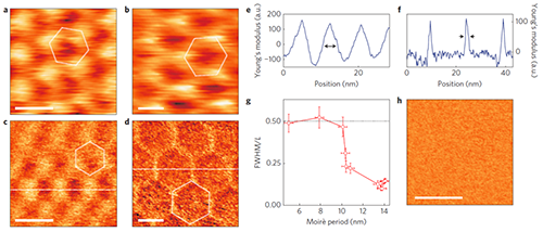 |
| Fig. 1 (A) Local resistance measured by conductive AFM for one of our graphene-on-hBN samples with an 8 nm moiré pattern. Colour scale: white to black is 105 kΩ to 120 kΩ. (B) Same as in (A) for a sample with a 14 nm moiré periodicity – the crystallographic axes of graphene and hBN are practically aligned. Colour scale: from 135 kΩ to 170 kΩ. (CandD) Young modulus distribution, measured in the PeakForce mode, for structures with 8 and 14 nm moiré patterns, respectively. (EandF) Cross-sections of the Young modulus distribution taken along the dashed line in (C) and (D), respectively, and averaged over 10 scanning lines (approx. 2.5nm). (G) Ratio between FWHM of the peak in the Young’s modulus distribution (as marked by dashed arrows in (E) and (F)) and the period of moiré structure L, as a function of the period of the moiré structure for several of our samples. (H) Young’s modulus distribution across an unaligned sample (angle between graphene and hBN ~15o). |
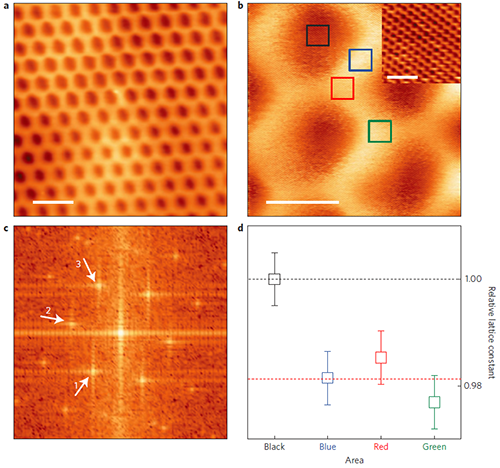 |
| Fig. 2 (A) STM image of one of our aligned samples. Moiré pattern is clearly visible. Scale bar 30nm. Sample bias -0.1V, tunnelling current 300pA. (B) Same as in (A), just under higher magnification. Both the moiré pattern and the atomic structure are resolved. Scale bar 10nm. Sample bias -0.1V, tunnelling current 800pA. Coloured squares (3nm in size) indicate the fragments used for Fourier transformation to determine the interatomic distance. (C) Example of the Fourier transformation of atomically resolved structure. In this case, as the starting image we used 3nm × 3nm square image at the vertex of the hexagonal pattern (red square in B). Scale bar 5nm-1. (D) Relative lattice constants (with respect to those measured for the area marked by black square in (B)) for different areas within the moiré pattern (colours corresponds to those in (B)). Obtained from the positions of the first order peaks in (C) and averaged over the three directions. |
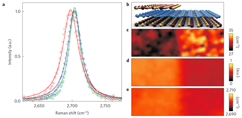 |
| Fig. 3(A)Raman 2D peak for various graphene samples on hBN samples. The data is normalised by the amplitude of the 2D peak. Symbols are the experimental data points, with lines of the corresponding Lorentzian fit in the respective colour. Red circles and line – for graphene on hBN with L 14 nm, non-encapsulated. Blue triangles and line – for the same L but encapsulated. Green squares and line - L 8 nm, non-encapsulated.(B)Schematic representation of one of our devices with graphene partially encapsulated.(C)Spatial map of the FWHM of 2D peak for a graphene on hBN sample with the period of moiré pattern 14nm. Left half of the sample is encapsulated with a few layers of hBN. Crystallographic directions of the top hBN are rotated by approximately 15°with respect to those of graphene.(D)Spatial map of the amplitude of the 2D peak for the same sample as in (C). Normalised to the amplitude of the G peak.(E)Spatial map of the position of the 2D peak for the same sample as in (C). Laser excitation is 488nm for all Raman data. |