Measurements of Graphene Intrinsic Carrier Properties Reveal Its Potentials as a Material for High Temperature Devices
Date:17-10-2014 Print
High temperature devices are demanded for military, astronautic, and heavy industry applications, where high power density is required or high temperature environment can’t be avoided. In order to make a nonlinear semiconductor device (p-n junction or transistor) functioning, the chemically doped carriers or the gating generated carriers have to be the controlling factor within the semiconductor material. However, when the device temperature increases, the semiconductor’s intrinsic carrier density will increase. Once the temperature reaches a certain point that, the semiconductor’s intrinsic carrier surpasses the chemical doping or gating effect and dominates the device’s response, the nonlinear device will simply fail its function. For instance, a Si device’s intrinsic carrier density will double if temperature increases 8 K from room temperature, the maximum operation temperature for a Si device is 250℃. Normally for a semiconductor, a larger band gap gives a higher operation temperature; however, a larger band gap also increases the difficulty of carrier density tuning. Graphene is semi-metallic, not a semiconductor. By a doping or field effect, graphene can be made into a p-n junction or a transistor as well. A significant amount of attention has been directed toward the room temperature and low temperature measurements in pursuing a high carrier mobility. However, little attention has been made to the role of intrinsic carriers in graphene, because the great ability of graphene to tolerate the impact of temperature masks the existence of its intrinsic carriers. Thus, the importance of graphene as a material for high temperature devices is not noticed.
Yan Yin, Li Wang and Kuijuan Jin at the Institute of Physics, Chinese Academy of Sciences, working together with Ying Fang’s team at National Center for Nanoscience and Technology and Wenzhong Wang at Minzu University of China, use a Raman method to measure the properties of intrinsic carriers and G mode phonon energies in a voltage biased graphene device up to 2400 K. We find the intrinsic Fermi level, |EF|=2.93kBT or intrinsic carrier density, nin=3.87×106 cm-2 K-2∙T2. The result tells us that a properly fabricated graphene p-n junction or transistor can operate well above 1500 K and will not fail until other parts melt. Working together with silicon carbide (SiC), graphene might be one of the building materials for coming high temperature devices. We also map out the three stage behavior of carrier drift velocity as a function of the field or temperature, and graphene shows a linear decline in “saturation” drift velocity in contrast to a constant saturation drift velocity in traditional semiconductor materials, as the result of the degeneracy of carriers and the Pauli exclusion principle. At the same time, we identify the G mode phonon intrinsic energy coefficients with temperature, ΩG=-4.596×10⁻⁶ cm-1 K-2 T2+-0.0139cm-1 K-1 T+1584 cm-1, which works up to 2400 K.
In summary, we use Raman method to quantitatively measure the graphene intrinsic carrier density, drift velocity and G mode phonon energy as functions of temperature up to 2500 K. We find that the intrinsic carrier density of graphene is an order of magnitude less sensitive to temperature than that of traditional semiconductor materials. We foresee graphene becomes a material for high temperature devices. We map out the three stage behavior of carrier drift velocity as a function of the field or temperature and find the G mode phonon intrinsic energy coefficients with temperature up to 2400K. All of above reveal the great potential of graphene as a foundational material for high temperature devices, identify a new research direction for graphene applications, and are vital in understanding the physics of graphene under high field or high temperature.
This work has been published in Scientific Report (Scientific Reports 4,5758 (2014);doi:10.1038/srep05758). This work was supported by the National Basic Research Program of China, by the Young Scientists Fund of the National Natural Science Foundation of China, by the National Natural Science Foundation of China, and by the Scientific Research Start-up Fund for the Returned Overseas Chinese Scholars from Ministry of Education of China. This work can be found at:http://www.nature.com/srep/2014/140721/srep05758/full/srep05758.html
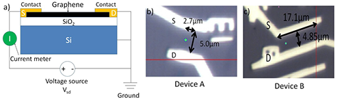 |
| Figure 1 | Graphene device information.a, The sketch of the stacking structure of the devices and the electrical measurement layout.b, Optical picture of the graphene device A.c, Optical picture of the graphene device B. The widths and lengths of the devices are marked in the pictures. The blue dots are the optical focus positions during the measurements of the devices. The letters D and S indicate the drain electrodes and source electrodes. |
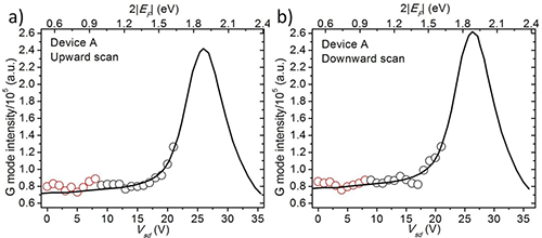 |
| Figure 2 | Measurement and fitting results for G mode intensities as a function of theVsd. a,Device A duringVsdupward scan.b, Device A duringVsddownward scan. We only use theVsd≥9 V data points for the fitting in order to give a better fitting weight for the high bias data points. The upper axis is for the Fermi level obtained from this fitting in the device. |
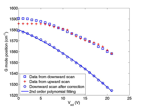 |
| Figure 3 | The G mode peak positions as a function of theVsdfor device A. The blue square, red cross, and blue circle data points are the experimental data points forVsddownward scan,Vsdupward scan, and the G mode position for downward scan after taking out the effect of carrier density, respectively. The blue curve is the fitting result for the corrected G mode position with a 2nd order polynomial function. |
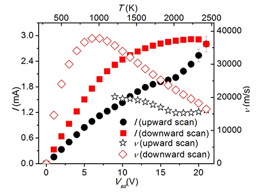 |
| Figure 4 | Device I-V curves, temperatures, and carrier drift velocities.The defect level is 4×1012cm-2. Red solid square points and black solid round points are the I-V data duringVsddownward and upward scan, respectively, using left y axis. The current values are the averages of the currents before and after the Raman measurements, the differences of the two are plotted as error bars. Red hollow diamond points and black hollow star points are calculated carrier drift velocities duringVsddownward and upward scan, respectively, using right y axis. The top axis plots the device temperature. |