High efficient photon-carrier extraction phenomenon in low dimensional semiconductors
Date:10-11-2016 Print
The light to electricity conversion is the fundamental of many modern semiconductor devices, such as solar cell and photon detector. The research on the subject is still active in order to boost the device performance. The use of low dimensional semiconductors in the light to electricity conversion is still difficult due to the possible quantum efficiency loss and thinner epitaxial thickness to avoid defects.
Recently, Wenqi Wang et. al. in Prof. Hong Chen group in in Institute of Physics, Chinese Academy of Sciences, collaborated with Prof. Wuming Liu’s group found a high efficient localized carrier extraction phenomenon in low dimensional semiconductor within the depletion region of PN junction.
As shown in Figure 1, around 88% the PL intensity of InAs/GaAs quantum dots quenched in the sample with a P-I-N structure during the short and open circuit condition under resonant PL tests. However, only slightly PL intensity change in a N-I-N structure was measured.
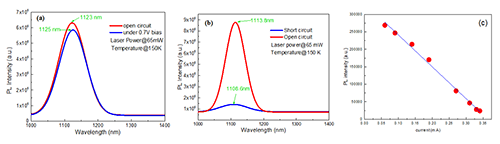 |
| Fig. 1. (a) resonant PL of n-i-n sample measured under open and -0.7V condition;(b) ) resonant PL of p-i-n sample measured under open and short circuit (zero bias) condition;(c)linear relationship between QD PL intensity and circuit current. The above mentioned phenomenon provides the possibility of fabricating novel high performance quantum well interband transition detector. A prototype interband transition of strained InGaAs/GaAs quantum wells was fabricated by the same team. The external quantum efficiency was measured to be 31% using only 100nm effective absorption thickness without an anti-reflection layer. Such high value leads to an absorption coefficient of 3.7×104cm-1which is obviously larger than previously reported values. The results here demonstrate the possibility of fabricating high performance and low cost infrared photon detectors. (in press) |