Control of Conduction Type and Construction of Novel Planar Devices Realized in Black Phosphorus
Date:27-12-2016 Print
The discovery of graphene has brought unprecedented opportunities to next-generation electronic devices which promise to extend the scaling limits in silicon-based complementary metal oxide semiconductor field-effect transistors (FETs). Although possessing an extremely high mobility (~20000 cm2/Vs), graphene lacks a bandgap, which is a hurdle for logic transistors. On the contrary, transition metal dichalcogenides, another widely investigated layered materials, possess a moderate and tunable (thickness-dependent) bandgap ranging from 0.4 to 2.3 eV. Field-effect transistors based on them have demonstrated current on/off ratios of 106-108 and excellent subthreshold swings (close to ideal value of 60 mV/decade). However, their mobility ranges from 10 to 200 cm2/Vs, restricting their applications in RF transistors.
As a young member in the family of two dimensional materials, black phosphorus (BP) has attracted great attention since its discovery. BP shows high hole mobility (~1000 cm2/Vs) and a sizable and tunable bandgap (0.3 eV for bulk and 2.0 eV for monolayer)., which meets the basic requirements for logic circuits applications. To realize a complementary logic operation, it needs to control the conduction type in BP FETs, i.e., the dominant carrier types, holes (P-type) or electrons (N-type). The absence of reliable substitutional doping techniques makes this task a great challenge.
Early in 2009, researchers in Prof. Hong-Jun Gao’s group in the Institute of Physics (IoP) successfully observed the atomically resolved surface structure of bulk black phosphorus by scanning tunneling microscope (STM), and characterized the geometrical and electronic properties (J. Phys. Chem. C, 113, 18823 (2009)) [1]. To effectively overcome the instability and control the conduction type of black phosphorus, recently, Ph. D. candidate Guocai Wang and Dr. Lihong Bao from Prof. Hong-Jun Gao’s group collaborate with Prof. Liling Sun, Prof. Guangyu Zhang, and Prof. Changzhi Gu from IoP, and Prof. Sokrates T. Pantelides from Vanderbilt University in USA. For the first time, they demonstrate that capping a thin BP layer with a cross-linked poly-methyl-methacrylate (PMMA) layer can modify the conductivity type of BP by a surface charge transfer process, converting a BP layer p-type to n-type. Combining BP films capped by cross-linked PMMA to a standard BP, a family of planar devices can be created, including BP gated diodes (rectification ratio >102), BP barristors (on/off ratio >105), and BP logic inverter (gain~0.75), which are capable of performing current rectification, switching, and signal inversion operations. The device performance demonstrated here suggests a promising route for developing 2D-based electronics.
As shown in Figure 1, when the channel of black phosphorus FET is partially capped with a layer of cross-linked PMMA, the transfer curve of the uncapped part shows a holes conduction dominated transport behavior (P-type), while that of the capped part shows an electrons conduction dominated transport, verifying the electron doping effect of cross-linked PMMA. Furthermore, through varying the electron beam dosage to irradiate the PMMA, the magnitude of doping could be effectively controlled. The combination of black phosphorus N-FET and P-FET in series results in the formation of black phosphorus gated diodes, which is confirmed by the output curves of the device. The rectification ratio is over 100 and could be modulated by varying the back gate voltage bias. Moreover, when the voltage bias is zero, the current reaches the orders of magnitude of pA/μm, indicating a complete OFF state and low power consumption of the device (Figure 2).
The above results show that by capping the different part of the channel in black phosphorus FET with cross-linked PMMA, electron conduction FET (fully capped and gated diodes (partially capped) could be created. When the strip of cross-linked PMMA is placed into the middle of the channel in BP FET, the output curve of the device under zero back gate voltage bias also shows a current rectification behavior. When the device is reversely biased, the device shows almost the same rectification behavior with that of forward bias, confirming the bidirectional current rectification capability of the device (Figure 3). Due to the electron conduction dominated transport in cross-linked PMMA capped region and hole conduction dominated transport in uncapped region, a potential barrier will be formed at their contact region and only the carrier gaining enough energy can pass though this barrier. Due to the symmetric configuration of the device, the bidirectional current rectification feature could be observed.
Logic inverter is the elementary device in logic circuits. The key to realize the logic operation of logic inverter is the availability of separate N-FET and P-FET devices and control of the conduction type in the host semiconductors. As shown in Figure 4, when the black phosphorus NFET and PFET are combined in series, a black phosphorus logic inverter can be constructed. The output characteristics of the device verifies its functionality of logic inverter and current gain is ~0.75. In ideal logic inverters, the current gain is an infinite value. The low current gain in our black phosphorus logic inverter is due to the fact that the transport in NFET and PFET are modulated by a common global back gate and a complete match state is quite difficult to be reached. To improve the current gain, separate gates are required to tune the transport of NFET and PFET separately. Using the high k dielectric is also a feasible option.
The work entitled “Introduction of Interfacial Charges to Black Phosphorus for a Family of Planar Devices” is recently published on Nano Letters 16, 6870 (2016) [2]. This work is financially supported by the Ministry of Science and Technology, the National Natural Science Foundation of China, and Chinese Academy of Sciences.
The links for the above results are:
[1] http://pubs.acs.org/doi/abs/10.1021/jp907062n
[2] http://pubsdc3.acs.org/doi/abs/10.1021/acs.nanolett.6b02704
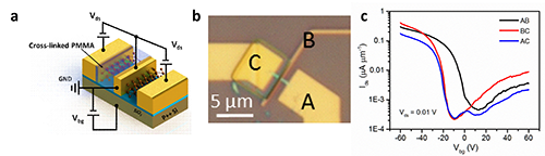 |
| Figure 1. (a) Schematic of BP FET devices with and without cross-linked PMMA as capping layer in the same channel and their measurement setup. The brown balls and sticks stand for the BP lattice. (b) Optical image of the device. (c) Transfer curve of pure BP FET (black curve, AB), cross-linked PMMA-covered BP FET (red curve,BC), and BP p−n diode (blue curve, AC). |
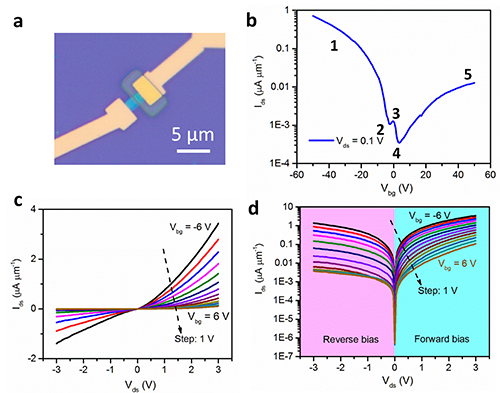 |
| Figure 2. (a) Optical image of BP p−n diode. (b) The forward diode current as a function of back gate voltages at constant source-drain bias of 0.1 V. (c) Current versus bias voltage under gate voltage modulation in the range of −6 to 6 V with a step of 1 V. (d) Logarithmic plot of the current−voltage characteristics in (c). The lowest current can reach 10−6μA μm−1, showing a completely “off” state. |
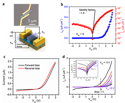 |
| Figure 3. (a) Optical image (upper panel) and schematic diagram (lower panel) of the device composed of two identical BP diodes in back-to-back series. (b) Output curve under both reverse and forward bias voltages at Vbg= 0. Fitting the logarithmic plot at small bias with Schockley’s equation yields an ideality factor of ~1.3. (c) Symmetric output curves. (d) Output curves under gate voltage modulation. Inset is the logarithmic plot. |
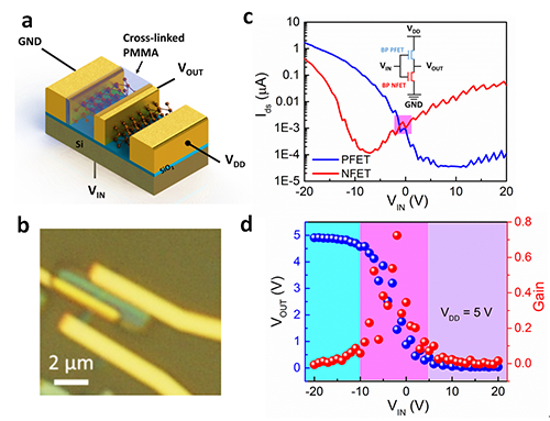 |
| Figure 4. (a) Schematic diagram of the logic inverter. (b) Optical image of the BP logic inverter. (c) Transfer characteristic of BP PFET and BP NFET realized by capping of cross-linked PMMA. (d) The output voltage and gain as a function of input voltage, showing a highest gain of 0.75 is obtained. The cyan-, pink-, and violet-shaded areas indicate three different working regimes of the BP logic inverter. |
Contact:
Institute of Physics
GAO Hong-Jun
E-mail: hjgao@iphy.ac.cn
Keywords:
Black phosphorus, interfacial charge, field-effect transistor, p-n diode, logic inverter
Abstract:
The capabilities to tune the conduction properties of materials by doping or electric fields are essential for the design of electronic devices. However, in two-dimensional materials substitutional doping has been achieved in only a few systems, such as Nb substitutional doping in MoS2. Surface charge transfer is still one of the popular ways to control whether the conduction is dominated by holes or electrons. Here, we demonstrate that a capping layer of cross-linked poly(methyl methacrylate) modifies the potential in a black phosphorus (BP) layer so that conduction in the absence of an external electric field is dominated by electrons, rather than holes. Using this technique to form adjoining regions dominated by hole and electron conduction, a family of novel planar devices, such as BP-gated diodes, BP bidirectional rectifier, and BP logic inverters, can be fabricated. The devices are potentially useful for electronic applications, including rectification and switching.
2. Room-Temperature, Low-Barrier Boron Doping of Graphene.pdf
3. Surface Structures of Black Phosphorus Investigated with Scanning Tunneling Microscopy.pdf
4. Introduction of Interfacial Charges to Black Phosphorus for a Family of Planar Devices.pdf