Interlayer-State-Coupling Dependent Ultrafast Charge Transfer in MoS2/WS2 Bilayers
Date:16-05-2017 Print
Since the discovery of graphene and the rise of MoS2, atomically thin two-dimensional (2D) crystals have grown into a huge family of materials ranging from semimetal, semiconductors to insulators. Monolayer transition-metal dichalcogenides denoted as MX2 (e.g., M =Mo, W, and X=S, Se, Te), have been prepared by physical exfoliation and chemical vapor deposition, providing more choices for 2D materials. The MX2 materials share similar crystalline structures and symmetries, but possess distinct electronic properties in band gaps and photoabsorption. The heterostructures vertically reassembled from different two-dimensional materials form even richer material systems, and thus provide a new platform for investigating new physics and exploring new applications. The heterostructures of two MX2 are of particular interests because many of them form type II heterojunctions, which facilitate the efficient separation of photo-excited electrons and holes and therefore exhibit great potentials in the applications of photodetectors, photovoltaic cells and light emitters.
Light-induced interlayer ultrafast charge transfer in two-dimensional heterostructures provides a new platform for optoelectronic and photovoltaic applications. Hong et al. firstly reports that collective motion of excitons at the interface leads to plasma oscillations associated with optical excitation in the ultrafast charge transfer in such van der Waals heterostructures, which provides a good insight in this new phenomenon (Hong et al. Nat. Nanotechnol. 2014, 9, 682). The charge separation process is generally hypothesized to be dependent on the interlayer stackings and interactions, however, the quantitative characteristics and detailed mechanism remain elusive.
Now a group from Institute of Physics, Chinese academy of sciences led by Prof. Sheng Meng demonstrates systematically the stacking-dependent interlayer charge transfer in MoS2/WS2 bilayer model system by first-principles time-dependent density-functional theory simulations. They show that the slight change in interlayer geometry can significantly modulate the charge transfer time from 100 fs to >1 ps scale. Detailed analysis further reveals that the transfer rate in MoS2/WS2 bilayers is governed by the electronic coupling between specific interlayer states, rather than interlayer binding strength, and follows a universal dependence on the specific-state-coupling strength. Their results establish the interlayer stacking as an effective freedom to control ultrafast charge transfer dynamics in 2D heterostructures, facilitating their future applications in optoelectronics and light harvesting.
This study entitled “Interlayer-State-Coupling Dependent Ultrafast Charge Transfer in MoS2/WS2 Bilayers” was published on Advanced Science.
The study was supported by the National Science Foundation, the Ministry of Science and Technology of China.
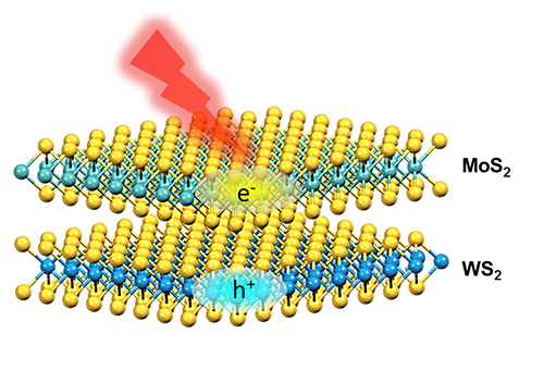 |
| Fig.1 Illustration of a MoS2/WS2 heterostructure and ultrafast charge dynamics.(Image by Institute of Physics) |
 |
| Fig.2 Hole transfer evolution for MoS2/WS2 in different stacking configurations. (Image by Institute of Physics) |
 |
| Fig.3 Interlayer-state-coupling dependent charge transfer rate in MoS2/WS2 bilayers. |
Contact:
Institute of Physics
Sheng Meng
Email:smeng@iphy.ac.cn
Key word:
interlayer-state-coupling, MoS2/WS2 heterostructures, stacking configurations, TDDFT calculations, ultrafast charge transfer
Abstract:
Slight changes in the interlayer configuration can significantly modulate ultrafast charge transfer time from 100 fs to >1 ps in MoS2/WS2 bilayer heterojunctions. Detailed analysis further reveals that the transfer rate is sensitively governed by the electronic coupling between specific interlayer states.