New method developed to construct intrinsically patterned two-dimensional materials for selective functionalization
Date:12-07-2017 Print
New method developed to construct intrinsically patterned two-dimensional materials for selective functionalization
Typically, application of 2D atomic crystals requires functionalization and patterning, for example, semiconductor films need to be doped as n-type or p-type in a lithographically-patterned way to construct pn junctions (light-emitting diodes, junction lasers, resistors) and transistor structures. Functionalization of 2D atomic crystals can be done in a variety of ways, e.g., by doping with impurities or molecules, either within the 2D lattices or adsorbed on the exposed surfaces.
Recently, Prof. Hong-Jun Gao’s group from Institute of Physics, Chinese Academy of Sciences reported the growth of a family of 2D atomic crystals that are intrinsically patterned and demonstrated that these materials can serve as templates for selective self-assembly of molecules or nanoclusters, as well as for the functionalization of the same substrate with two different species. They reported two prototypes of patterned 2D atomic crystals: 1H/1T monolayer PtSe2 tiling pattern and monolayer CuSe with periodic nanopores. In both patterned materials, adsorption of different species at preferred pattern components has been achieved, illustrating the potential for selective/dual functionalization.
Monolayer PtSe2 has two conformations: octahedral (1T) and triangular (1H). In 2015, Gao’s group successfully fabricated high-quality, single-crystalline, monolayer PtSe2 (1T) films by a single step of direct selenization of a Pt(111) substrate. [Nano Lett. 15, 4013 (2015)]. Based on this work, they constructed the 1H/1T patterned PtSe2 form (Figure 1 and Figure 2). In addition, the reversible transformation from 1H/1T-PtSe2 to 1T-PtSe2 has been successfully achieved by tuning the density of vacancies. The highly ordered triangular tiling patterns constructed by 1H and 1T phases of a monolayer PtSe2 make it a suitable template for selective adsorption of different species. Figure 2h and 2i shows that pentacene molecules adsorb selectively on 1H triangles, allowing the formation of a periodic array of molecules.
In addition to 1H/1T patterned PtSe2, Gao’s group fabricated an intrinsically patterned form of monolayer CuSe by direct selenization of Cu(111) substrate for the first time. Monolayer CuSe film with a honeycomb lattice is a new type of two-component 2D atomic crystal. To relieve the strain coming from lattice-mismatch between CuSe layer and Cu(111) substrate, monolayer CuSe has periodic arrays of identical triangular nanopores. By a combination of density functional theory (DFT) calculations and scanning tunneling microscopy (STM), they demonstrated that the nanopores are formed by removal of 13 atoms on CuSe lattice (three complete six-member rings) (Figure 3). To functionalize the patterned CuSe monolayer with nanopores, Fe atoms and FePc molecules are deposited on a CuSe monolayer. They found that Fe atoms form W-shape clusters in the nanopores with a formula of Fe13Se7 and FePc molecules are monodispersed and adsorbed only on CuSe terraces (Figure 4).
In addition, two intrinsically patterned monolayers (1H/1T-PtSe2 and CuSe) are stable in ambient conditions, which make these patterned monolayers suitable for applications involving ambient conditions.
This work entitled “Intrinsically patterned two-dimensional materials for selective adsorption of molecules and nanoclusters” was published on Nature Material with a News and Views entitled “CHALCOGENIDE-BASED 2D MATERIALS Intrinsic nanoscale patterning” in the same issue. “A method to realize regular patterns with nanometre precision during the synthesis of PtSe2 and CuSe monolayers has been developed”, said Prof. Joseph W. Lyding from University of Illinois at Urbana-Champaign. “The generalization to a very broad class of chalcogenide-based 2D materials will create further opportunities for fabricating nanoscale devices and chemical processing systems using the intrinsic nanoscale patterning processes demonstrated by Gao and colleagues.”
The work was mainly supported by the National Science Foundation, the Ministry of Science and Technology of China and Chinese Academy of Science.
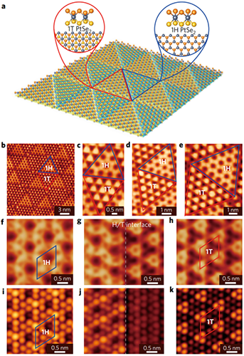 |
| Figure 1 | Schematics, STM images and STM simulations of 1H/1T tiling pattern in monolayer PtSe2. |
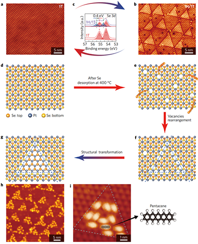 |
| Figure 2 | Reversible transition and selective adsorption of 1H/1T tiling pattern. |
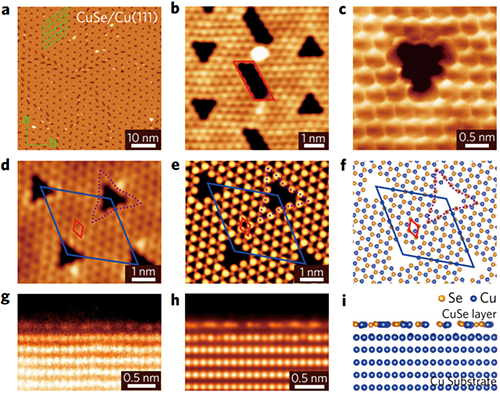 |
| Figure 3 | STM images, STEM images, model and simulations of patterned CuSe monolayer with periodic nanopores. |
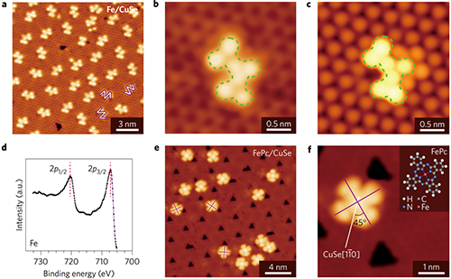 |
| Figure 4 | Selective adsorption of iron and FePc molecules on patterned CuSe with periodic nanopores. |
Contact:
Institute of Physics
GAO Hongjun
Email:hjgao@iphy.ac.cn
Keyword:
2D atomic crystals; Intrinsic pattern; functionalization;
Abstract:
The growth of a family of 2D materials that are intrinsically patterned has been achieved. Scanning tunneling microscope studies show the adsorption of different species at preferred pattern sites, demonstrating that these materials can serve as templates for selective self-assembly of molecules or nanoclusters, as well as for the functionalization of the same material with two different species.