Scientists create atomic scale, two-dimensional electronic Kagome lattice in silicene
Date:15-11-2018 Print
Scientists from the Institute of Physics (IOP) at Chinese Academy of Sciences, working with colleagues at University of Wollongong (UOW) in Australia, Beihang University, and Nankai University (NKU), have successfully created an atomic scale, two-dimensional electronic Kagome lattice in multilayer silicene, which has potential applications in electronics and quantum computing.
A Kagome lattice is named after a traditional Japanese woven bamboo pattern composed of interlaced triangles and hexagons. Scientists have long been interested in making a 2D Kagome lattice because of the useful theoretical electronic properties such a structure would have. The electrons, instead of flowing through, would instead turn around in a vortex and would become locked in the lattice. When the lattice is broken, for example an edge forms, combined with spin-orbital coupling effect, novel quantum phenomena, such as frictional quantum Hall effect, are expected to happen at room temperature. This will pave a way for quantum devices in the future. However, in nature, few materials can host such promising lattice, and creating such a material has proved extremely challenging.
Recently, Prof. Lan Chen from IOP, cooperated with Prof. Y. Du in UOW and Prof. Z. P. Hu in NKU, created the 2D electronic Kagome lattice by layering and twisting two nanosheets of silicene. Silicene is a silicon-based, one-atom thick, Dirac fermion material with a hexagonal honeycomb structure, which electrons can speed across at close to the speed of light. When silicene is twisted into a Kagome lattice, however, electrons become "trapped", circling around in the hexagons of the lattice. An flat band peak forms in the density of states. A robust and pronounced one-dimensional edge state has been revealed at the Kagome edge.
The expected benefits of this breakthrough will be much more energy efficient electronic devices and faster, more powerful computers.
This study entitled “Realization of flat band with possible nontrivial topology in electronic Kagome lattice” was published in Science Advances on 16 November 2018.
This work was supported by the National Science Foundation, the Ministry of Science and Technology of China, the Chinese Academy of Sciences and Australian Research Council (ARC).
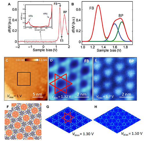
Fig. 1. Atomic and electronic structures of the electronic Kagome area on multilayer silicene. (Image by Institute of Physics)
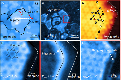
Fig. 2 Edge states of electronic Kagome area. (Image by Institute of Physics)
Contact:
Institute of Physics
Lan Chen
Email:lchen@iphy.ac.cn
Key word:
Kagome lattice; silicene; flat band; scanning tunnelling microscopy
Abstract:
Destructive quantum interference in a frustrated Kagome lattice with only nearest-neighbor hopping will result in a discrete flat band (FB) without any dispersion. An FB with possible nontrivial topology in an electronic Kagome lattice was experimental realized on twisted multilayer silicene.