Enhancing charge density waves by Moiré engineering in 1T-TiTe2/1T-TiSe2 heterostructures
Date:20-12-2021 Print
When stacking two layers of van der Waals (vdW) materials, a moiré pattern is produced by the modulation of the long wavelength periodic potential. The moiré pattern is a promising means in engineering both the atomic geometry and electronic structure. A variety of emergent phenomena have been discovered in twisted vdW bilayers of graphene or semiconducting transition-metal dichalcogenide (2H-TMD), however, little is known about the twisted bilayer of metallic 1T-TMD materials.
Recently, research teams led by Prof. Shao-Chun Li at Nanjing University (NJU) and Prof. Sheng Meng at Institute of Physics (IoP), Chinese Academy of Sciences, have discovered for the first time that the many-body effects, particularly the electronic quantum correlation, can be tuned in metallic vdW monolayers through moiré engineering.
They found that in 1T-TiTe2/1T-TiSe2 heterostructures, when the twist angle θ is near ~0.5°, the profound 2×2 charge density wave (CDW) domains are formed in 1T-TiTe2. The CDW domains are trapped in the moiré pattern and separated by the 1×1 normal-state regions. This CDW state is significantly enhanced to persist even at room temperature. However, in larger twist angles, such moiré-trapped CDW patterns were not observed. Using first-principles calculations within the framework density functional theory, they demonstrated that the formation of moiré-trapped CDW state can be ascribed to the local strain variations due to atomic reconstructions modulated by moiré patterns. This study paves a new way to constructing metallic twisted vdW bilayers and tuning the many-body effects via moiré engineering.
This study entitled "Moiré enhanced charge density wave state in twisted 1T-TiTe2/1T-TiSe2heterostructures" was published on Nature Materials.
The study was supported by the National Natural Science Foundation of China and the Chinese Academy of Sciences.
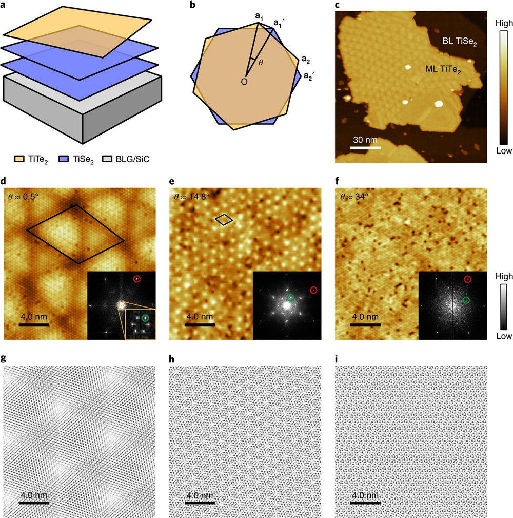
Fig.1 Scanning tunneling microscopy (STM) topographic images of various moiré patterns with different twist angles. (Image by NJU)
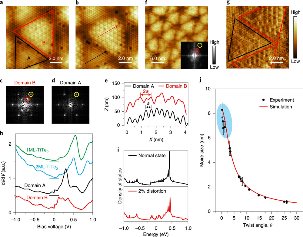
Fig.2 Moiré enhanced CDWs near 0°. (Image by NJU and IoP)
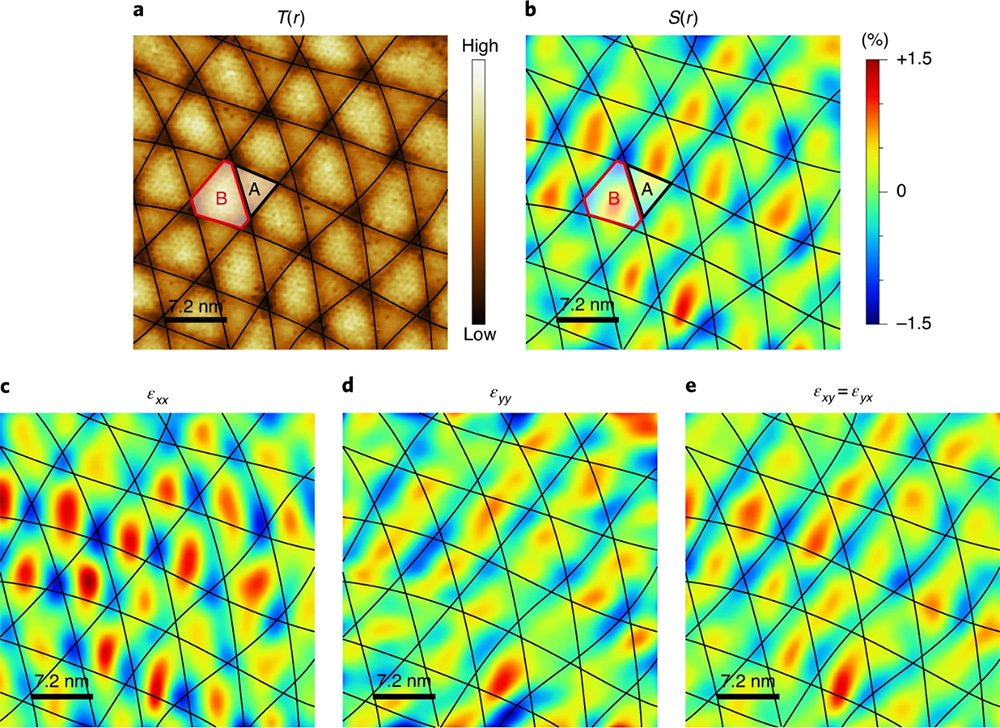
Fig.3 Symmetric strain map. (Image by NJU)
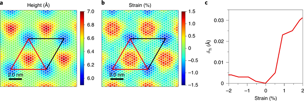
Fig.4 Relative height and strain field of the heterostructures. (Image by IoP)
Contact:
Institute of Physics
MENG, Sheng
Email: smeng@iphy.ac.cn
Nanjing University
LI, Shaochun
Email: scli@nju.edu.cn
Key word:
Moiré; CDWs;
Abstract:
Nanoscale periodic moiré patterns, formed at the interface of twisted (or lattice mismatch) bilayer of two-dimensional materials, provide a new degree of freedom for engineering the electronic properties of van der Waals (vdW) heterostructures. A variety of emergent phenomena have been recently discovered in twisted vdW bilayers of graphene or semiconducting transition-metal dichalcogenide (2H-TMD). However, the twisted bilayer of metallic 1T-TMD materials has not yet been explored so far. Indeed, the individual 1T-TMD layers themselves exhibit rich many-body effects. In this work, we constructed the epitaxial bilayer of 1T-TiTe2/1T-TiSe2 with various twist angles by using molecular beam epitaxy, and investigated the moiré pattern induced/enhanced charge density wave states with scanning tunneling microscopy. As the twist angle θ is near ~0.5o, surprisingly, the profound 2×2 charge density wave (CDW) domains are formed in 1T-TiTe2, as separated by the 1×1 normal-state ones, and trapped in the moiré pattern. The formation of moiré-trapped CDW state can be ascribed to the local strain variation due to atomic reconstruction. Furthermore, this CDW state is significantly enhanced to persist at room temperature, feasible to future CDW-based applications. Such moiré-trapped CDW patterns were not observed in larger twist angles. This study paves a new way to constructing metallic twist vdW bilayers and tuning the many-body effect via moiré engineering.