Realization of ultrahigh-speed (~ 20 ns) non-volatile memory devices
Date:04-05-2021 Print
The development of high-performance memory devices has played a key role in the innovation of modern electronics. It is critical to develop ultrafast and non-volatile memory devices driven by the explosive growth of massive data storage and desire of ultrafast data processing. Current bottleneck in the memory field includes operation speed, data retention, endurance and extinction ratio. In particular, while the scaling of devices continues, silicon-based technology will soon reach a critical limit to meet the increasing demands for memory capacity. One of the key challenges is related to the unavoidable interfacial dangling bonds in ultrathin-body silicon, which causes substantial degradation in device performance. It is thus an urgent need to seek atomically sharp interfaces and integrate them seamlessly into the device architecture.
Among all of candidates, the emerging two-dimensional (2D) materials and their heterostructures represent ideal atomically flat in-plane surfaces potentially free from surface dangling bonds and are immune to short-channel effects that can allow effective electrostatic control and mechanical flexibility. Indeed, a few examples employing 2D materials for flash memory devices have been recently attempted but with limited device performance. For example, a very long write time on order of milliseconds to seconds was observed in the 2D materials based floating-gate memory devices, while alternative semi-floating-gate configurations have shown improved write time (nanoseconds) but extremely short retention time in the range of seconds, making them unsuitable for long-term storage. Theoretically, an ideal floating-gate memory devices based on planar layer materials should allow nanosecond order operational time, but the ultrahigh-speed floating-gate memory has not yet been reported so far.
Recently, a research team led by Prof. Hong-Jun Gao at IoP, CAS, has demonstrated for the first time that ultrahigh-speed, nonvolatile floating-gate memory devices can be achieved without the need to modify commercial device architecture by employing 2D van der Waals heterostructures with improved interfacial coupling and atomically sharp interfaces. In particular, ultrahigh-speed operation with nanosecond write and read times that is limited by instrumentation response, extremely high extinction ratio of 1010, and a 10-yr retention time have been successfully achieved.
Fig. 1a and 1b show the schematic and optical photograph of the device, in which InSe is the channel, hBN is tunnel layer, multilayered graphene (MLG) is floating gate, SiO2 is the control gate, and heavily doped Si is the control gate electrode, respectively. Atomically resolved high-resolution scanning tunneling electron microscopy characterization shows that the InSe/hBN/MLG heterostructure possesses atomically sharp interfacial characteristics. Fundamental memory characterization on the floating-gate transistor indicates a large memory window (Fig. 2). When applying a pulse voltage with amplitude of +17.7/-17.7 V and full width at half maximum of 160 ns to perform programming/erasing operations, the floating-gate memory shows an ultrahigh extinction ratio (~1010), extremely long retention time (> 10-yr), and superior endurance (over 2000 times repeated programming/erasing) (Fig. 3). Furthermore, using the home-built super-short pulse source (~21 ns of FWHM and +20.2/-20.8 V of amplitude) to program/erase the device, ultrahigh extinction ratio (~1010) and ultrafast readout can also be successfully achieved (Fig. 4 a-d). When the channel materials is replaced by MoS2, ultrahigh-speed program/erase operation can also be successfully obtained, indicating the universality of the ultrahigh-speed operations in the van der Waals heterostructure with atomically sharp interfaces. Benefit from the ultrahigh extinction ratio, multi-bit storage can be achieved by optimizing the thickness of hBN (Fig. 4e).
Floating-gate memory devices based on van der Waals heterostructure with atomically sharp interface have comparable program speed with dynamic randomly accessed memory (DRAM), and simultaneously possessed non-volatile and large storage capacity. This is important for developing future high-performance non-volatile memory devices and provides an alternative route for the development of high-performance electronic devices based on van der Waals heterostructure. The main challenge for further application lies in the epitaxial growth of high-quality and large-scale hBN and two-dimensional atomic crystal materials and its device integration.
The above results have been published on Nature Nanotechnology (2021) entitled with "Atomically sharp interface enabled ultrahigh-speed, nonvolatile memory device". Liangmei Wu (IoP), Aiwei Wang (IoP), Jinan Shi (UCAS), and Jiahao Yan (IoP) are equally contributed to this work. Corresponding authors include Dr. Lihong Bao, Prof. Min Ouyang, and Prof. Hong-Jun Gao. This work is supported by National Key Research & Development Projects of China (Grant No. 2016YFA0202300 & 2018FYA0305800), National Natural Science Foundation of China (Grant Nos. 61888102), Strategic Priority Research Program of Chinese Academy of Sciences (CAS, Grant No. XDB30000000, XDB28000000), and Youth Innovation Promotion Association of CAS (Y201902).
This paper is available at:
https://dx.doi.org/10.1038/s41565-021-00904-5

Fig. 1 | Atomically sharp interfaces embedded in nonvolatile memory device with floating-gate configuration built upon van der Waals heterostructures.

Fig. 2 | 2D InSe based floating-gate memory device with large memory window.

Fig. 3 | Programming and erasing nonvolatile InSe floating-gate memory devices with large extinction ratio and robust performance. a, Schematic energy-band diagrams of a memory device for programming, reading and erasing operations. b, The conductance of the InSe channel can be toggled between low-conductance state (i.e. program state) and high-conductance state (i.e. erase state) by applying a single +17.7 V or -17.7 V voltage pulse with 160 ns FWHM, respectively. c, Time variation of threshold voltage after +17.7/-17.7 V programming/erasing pulses with 160 ns FWHM. d, Endurance performance test of the memory device executed with alternative voltage pulses (+17.7/-17.7 V programming/erasing pulses with 160 ns FWHM).
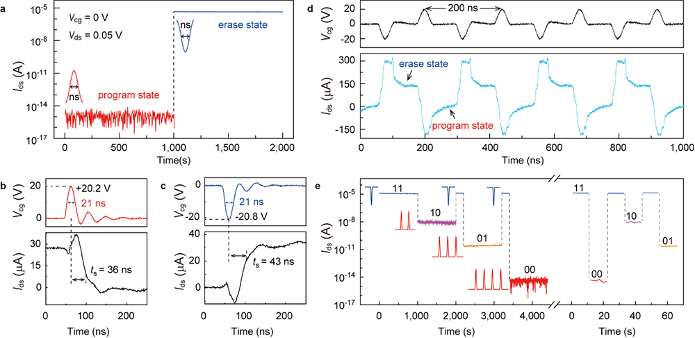
Fig. 4 | Ultrafast operation of memory cell and enabled multi-bit storage paradigm. a, The InSe memory cell with 10.0-nm-thick hBN layers can be successfully programmed/erased by a positive/negative voltage pulse with nanosecond pulse width, while maintaining high extinction ratio of 1010. The amplitude of voltage pulse is +20.2 V/-20.8 V. b,c, Ultrafast response of memory cells after programming (b) and erasing (c) pulses. d, Demonstration of ultrahigh frequency operation by sequential programming and erasing pulses with ~100 ns intervals. e, Realization of reproducible multi-bit storage from devices with 12.0-nm-thick hBN layers by a simple combination of ultrafast pulse sequence, with an example of repeatable 2-bit memory capacity demonstrated in the figure. By designing and applying sequential pulses for data programming, multiple level states of the memory cell can be programmed with discernible extinction ratio to achieve multi-bit storage. All programmed states can be consistently erased by a single nanosecond negative voltage pulse. The voltage amplitude and FWHM of programming and erasing pulses are (+20.2 V, 21 ns) and (-20.8 V, 21 ns), respectively.