More is better: epitaxial multilayer MoS2 wafers promise high-performance transistors
Date:13-06-2022 Print
Two-dimensional (2D) semiconductors, such as MoS2, enable the unprecedented possibilities to solve the bottleneck of transistor scaling and to build novel logic circuits with faster speed, lower power consumption, flexibility and transparency, benefiting from their ultra-thin thickness, dangling-bond-free flat surface and excellent gate controllability. In 2015, International Technology Roadmap for Semiconductors (ITRS) clearly pointed out that 2D semiconductors are key materials for next-generation high-performance devices. In 2021, Intel listed 2D MoS2-based transistor technology as one of the three breakthrough technologies for the next decade.
Tremendous efforts have been devoted to exploring the scaled-up potentials of monolayer MoS2, including both wafer-scale synthesis of high-quality materials and large-area devices. For instance, 4-inch wafer-scale monolayer MoS2 with large domain sizes (up to ~300 μm) and record-high electronic quality (average field-effect mobility of ~80cm2·V-1·s-1) has already been demonstrated via van der Waals epitaxial growth (Nano Lett. 2020; 20: 7193).
In terms of a further improvement of the electronic quality of the large-scale monolayer MoS2, structural imperfections should be eliminated as much as possible; however, there is not much space left for monolayer MoS2 after ten years of synthesis optimizations in this field. Another key direction is to switch to multilayer MoS2, e.g., bilayers and trilayers, since they have intrinsically higher electronic quality than monolayers and thus are conducive to higher-performance devices and logic circuit. However, due to the fundamental limitation of thermodynamics, it is still a great challenge to realize wafer-scale multilayer MoS2 with high-quality and large-scale uniformity.
Recently, Zhang Guangyu’s group from Beijing National Laboratory for Condensed Matter Physics and Institute of Physics, Chinese Academy of Sciences has overcome the fundamental limitations of thermodynamics by exploiting the proximity effect of sapphire (0001) substrate and achieved, for the first time, the growth of high-quality multilayer MoS2 4-inch wafers via the layer-by-layer epitaxy process. The epitaxy leads to well-defined stacking orders between adjacent epitaxial layers and offers a delicate control of layer numbers up to 6.
Compared to monolayers, thicker-layer MoS2 field-effect transistors show significant improvements in device performances. For long-channel devices (channel-length of 5 to 50 μm), the average field-effect mobility at room temperature can increase from ~80cm2·V-1·s-1 for monolayers to ~110/145cm2·V-1·s-1 for bilayer/trilayer devices, improved by 37.5%/81.3%. Considering that, in well-developed thin-film transistors (TFTs), field-effect mobility is 10-40cm2·V-1·s-1 for indium–gallium–zinc-oxide TFTs and 50-100cm2·V-1·s-1 for low-temperature polycrystalline silicon TFTs, the excellent average field-effect mobility of >100cm2·V-1·s-1 strongly uncovers a great potential of bi- and tri-layer MoS2 films for high-performance TFT applications. In addition, for trilayer MoS2 field-effect transistors, the highest room temperature mobility can reach up to 234.7cm2·V-1·s-1, setting a new mobility record for devices based on 2D transition-metal sulfide semiconductors.
For devices with channel-length of 100 nm, the current density (Vds=1 V) is increased from 0.4 mA·μm-1 for monolayer to 0.64/0.81 mA·μm-1 for bilayer/trilayer, showing an enhancement factor of 60%/102.5%. Remarkably, for 40 nm short-channel devices, a record-high on-current densities of 1.70/1.22/0.94 mA/μm at Vds=2/1/0.65 V, as well as a high on/off ratio exceeding 107, are achieved in trilayer MoS2 field-effect transistors. Such high on-current density of trilayer MoS2 devices outperforms the previous state-of-the-art MoS2 transistors and also exceeds the target of high-performance logic transistors from the International Roadmap for Devices and Systems (IRDS) 2024, moving a step closer to practical applications of 2D MoS2 in electronics and logic circuits at sub-5 nm nodes.
This study entitled "Layer-by-layer epitaxy of multilayer MoS2 wafers" was published on National Science Review.
The study was supported by the National Key R&D Program (2021YFA1202900), the Strategic Priority Research Program of Chinese Academy of Sciences (CAS) (XDB30000000), the Key-Area Research and Development Program of Guangdong Province (2020B0101340001), the National Science Foundation of China (11834017 and 61888102), and the Key Research Program of Frontier Sciences of CAS (QYZDB-SSW-SLH004).
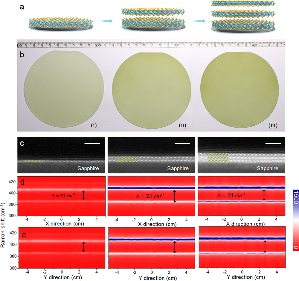
Fig.1 Layer-by-layer epitaxy of high-quality multilayer MoS2 4-inch wafers. (Image by Institute of Physics)
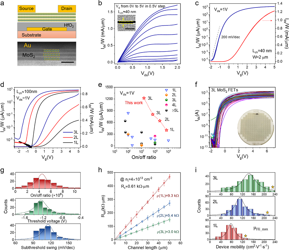
Fig.2 Bench-mark electronic quality of multilayer MoS2 field-effect transistors. (Image by Institute of Physics)
Contact:
Institute of Physics, Chinese Academy of Sciences
Zhang Guangyu
gyzhang@iphy.ac.cn
Key words:
2D semiconductor, Multilayer MoS2 wafer, layer-by-layer epitaxy, high performance transistors, thin film transistors
Abstract:
The layer-by-layer epitaxy of 4-inch multilayer MoS2 wafers are achieved. Compared with monolayers, device performances of thicker-layer MoS2 are significantly improved. The average field-effect mobility increases from ~80cm2·V-1·s-1 for monolayers to ~110/145cm2·V-1·s-1 for bilayer/trilayer devices. The highest mobility of 234.7cm2·V-1·s-1 and a record-high on-current densities of 1.70 mA/μm are achieved in trilayer MoS2 devices, outperforming the target of IRDS 2024.