Flexible monolayer MoS2 integrated circuits with low power and high performance
Date:29-06-2023 Print
Flexible electronics plays an integral role in a large spectrum of fields including information technology, energy generation and storage, biosensing, and diagnosis. Among them, flexible integrated circuits (ICs) dealing with information processing are favorable in portable, wearable, and implantable electronics with technological demands towards flexibility and robustness of large-area devices.
Compared to conventional materials (e.g., organic semiconductors, silicon of either amorphous or polycrystalline forms), the emergent two-dimensional (2D) semiconductor of monolayer MoS2 shows great advantages for large-area flexible ICs with low power and high performance, because of its atomic thickness, dangling-bond-free flat surface, high electron mobility, mechanically strong (in-plane) and flexible (out-of-plane). However, despite extensive efforts, flexible monolayer MoS2 integrated circuits still suffer from either low performances or high-power consumptions, and it is challenging to realize both in a synergic manner.
Researchers from the Institute of Physics, Chinese Academy of Sciences have now demonstrated the realization of large-area flexible monolayer MoS2 ICs with low power and high performance by developing an ultra-thin high-κdielectric/metal gate fabrication technique. For 500 randomly picked flexible monolayer MoS2 transitions, the device yield is >96%; mobility averages at ~70 cm2·V-1·s-1 (maximizes at >110 cm2·V-1·s-1); on/off ratio averages at 5 × 10⁷ (maximizes at 1 × 10⁹) and subthreshold swing averages at ~83 mV·dec-1. Large-area flexible monolayer MoS2 ICs show excellent spatial uniformity with fully functional inverters, logic gates, and ring oscillators operating reliably under supply voltages below 1 V. The power consumption of an inverter can be as low as 10.3 pW·μm-1 at Vdd = 1 V.
'The realization of large-area flexible monolayer MoS2 ICs with low power and high performance represent a key step towards high-end applications of next-generation integrated portable, wearable, and implantable electronics', says Prof. Zhang Guangyu from the Institute of Physics, Chinese Academy of Sciences, the corresponding author of the work.
This study entitled "Low power flexible monolayer MoS2 integrated circuits" was published in Nature Communications.
The study was supported by the National Key Research and Development Program, the Strategic Priority Research Program of Chinese Academy of Sciences, the National Science Foundation of China, and the Key-Area Research and Development Program of Guangdong Province.
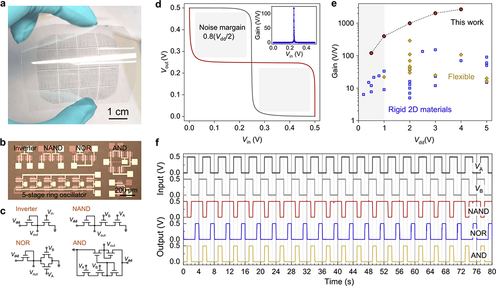
Fig.1 Flexible monolayer MoS2 integrated circuits. (Image by Institute of Physics)
Contact:
Institute of Physics
Zhang Guangyu
Email:gyzhang@iphy.ac.cn
Key words:
Monolayer MoS2; flexible integrated circuits; low power; high performance
Abstract:
Monolayer molybdenum disulfide (ML-MoS2) is an emergent two-dimensional (2D) semiconductor holding potential for flexible integrated circuits (ICs). The most important demands for the application of such ML-MoS2 ICs are low power consumption and high performance. However, these are currently challenging to satisfy due to limitations in the material quality and device fabrication technology. In this work, we develop an ultra-thin high-κdielectric/metal gate fabrication technique for the realization of thin film transistors based on high-quality wafer scale ML-MoS2 on both rigid and flexible substrates. The rigid devices can be operated in the deep-subthreshold regime with low power consumption and show negligible hysteresis, sharp subthreshold slope, high current density, and ultra-low leakage currents. Moreover, we realize fully functional large-scale flexible ICs operating at voltages below 1 V. Our process could represent a key step towards using energy-efficient flexible ML-MoS2 ICs in portable, wearable, and implantable electronics.