Recent STM Studies of Gate-tunable 2D Material Devices
Date: 2018-07-09
Time: 10:00
Venue: 物理所A楼三层会议室
Speaker: Jiong Lu
1 Department of Chemistry, National University of Singapore, 3 Science Drive 3, 117543
2 Centre for Advanced 2D Materials, National University of Singapore, Singapore 117546
Abstract:
2D materials with reduced dimensionality exhibit unprecedented tunability in both their electronic and optical, chemical properties due to the high susceptibility to the doping and the change of many-electron effects. BP is one of the few two-dimensional materials where it is possible to tune the bandgap over a wide energy range from the visible up to the infrared. Here we demonstrated a giant Stark effect in few-layer BP via electrostatic gating. Using low-temperature scanning tunnelling microscopy (LT-STM), we observed that a monotonic reduction of the bandgap of few layer BP occurs after the injected electrons compensate the existing defect-induced holes. Eventually, we achieved up to 35.5% bandgap modulation in the light-doping regime. When probed by STM spectroscopy, the local density of states in few-layer BP shows characteristic resonance features arising from layer-dependent sub-band structures due to quantum confinement effects. The demonstration of an electrical field tunable bandgap in BP paves the way to designing electro-optic modulators and photodetector devices that can be operated in a wide electromagnetic spectral range. We also employed LT-STM to probe the charge state of shallow acceptors in black phosphorus together with an aim to understand the spatial structures of bound hole states near individual acceptors. Our findings open up the new avenue for the investigation into charge transport through single dopants in gated BP nanodevices. In the last part of my talk, I will discuss about new experiments that involve the exploration of individual and self-assembled molecules adsorbed onto the surface of a back-gated graphene device. The back-gated graphene device substrate is unique for single-molecule surface investigations in that it can be electrostatically gated, thus changing and manipulating the charge-state of the supported molecules. Understanding the charge transfer and the resulting electronic structure at molecule/2D materials interface is essential for tuning the electronic and magnetic characteristics of such hybrid devices.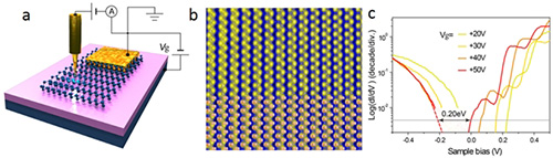
Fig 1. (a) Schematic illustration of a back-gated few-layer BP device (b) STM imaging of atomic lattice in BP. (c) Field tunable bandgap measured by local STM spectroscopy.
Reference
(1) Nature communications 7, 13553, 2016
(2) Nano letters 17 (11), 6935, 2017
(3) Nano Letters 17 (3), 1970, 2017
(4) Nature Nanotechnology 2018
Brief bio:
Dr. Jiong Lu is currently an assistant professor at Department of Chemistry, Centre for Advanced 2D Materials, at National University of Singapore (NUS). He received his Bachelor’s degree from Fudan University (China) in 2007 and Ph.D. degree from Department of Chemistry at NUS in 2011. After that, he worked as a postdoc fellow in Graphene Research Centre, NUS and then joined Mike Crommie’s group at Department of Physics, UC, Berkeley for his postdoctoral research. His current research interests include atomic-scale imaging and characterization of 2D materials and their gate-tunable devices, single-atom and atomically-precise metal clusters catalysis for energy related applications.
报告联系人:王业亮(82648072)