Unveil the Voltage-Controlled Magnon Transistor
Date:19-02-2024 Print
Magnons, as the elementary excitations in magnetically ordered systems, are quasi-particles capable of carrying both angular momentum and phase information. They serve as ideal information carriers for the development of wave-based computing and Joule-heating-free microelectronic devices. The efficient manipulation of magnon flows, as the foundational technology for integrated magnonic circuits, has thus become a focal topic in the field of magnonics. The pursuit of efficient magnon transistors has been pioneered using magnetic fields, microwaves, stress and direct current. However, the nonlocality or significant energy consumption of the above methods hampers their usages as applicable gating sources for magnonic devices. The voltage gating method featured by its locality, low energy consumption and high CMOS and LSIC compatibility, become the optimal strategy for constructing magnon transistors. Nevertheless, the electrical neutrality of magnons hinders their direct coupling with electric fields, posing a long-term challenge in the field of magnonics for the construction of voltage-gated magnon transistors.
M02 research group from the National Key Laboratory of Magnetism at the Institute of Physics Chinese Academy of Sciences, based on over a decade of magnonics studies, recently proposed an innovative solution to voltage control of magnon current. They theoretically demonstrated the physical principles of voltage-controlled magnon flow via tuning interfacial s-d coupling and experimentally inventing such a voltage-gated magnon transistor.
The proposed voltage-controlled magnon transistor was based on a non-magnetic metal/magnetic insulator/non-magnetic metal (NM/MI/NM) sandwich structure, with the bottom and top NM electrodes serving as the source and drain of the transistor, respectively. An \(\widehat{\mathbf{x}}\) directional charge current in the source electrode is converted into a \(\widehat{\mathbf{z}}\) directional spin current due to the spin Hall effect. At the NM/MI interface angular momentum is then transferred from conduction electrons in NM to the local magnetic moment in MI via interfacial s-d coupling, thus magnons activated. The produced magnons, driven by its density gradient, flows along the \(\widehat{\mathbf{z}}\) direction, forming a magnon spin current which is then converted into an \(\widehat{\mathbf{x}}\) directional electrical signal detected at the drain NM through the reverse spin Hall effect finally. A gating voltage at the NM/MI interface modulates the s-d coupling strength, thereafter influencing the spin-to-magnon conversion. In experiments, the efficiency of the magnon mediated electric current drag effect (or magnon current in Y3Fe5O12) in the Pt (8)/Y3Fe5O12 (80)/Pt (5 nm) magnon transistor can be controlled by applying a gate voltage between the top and bottom Pt electrodes. The controlling efficiency reaches 10%/(MV/cm), and the energy efficiency of magnon control by voltage is improved by 5 orders of magnitude compared to the previously reported direct current control methods. This prototype magnon transistor provides a novel solution for effective controlling of magnon transmission through gate voltage.
This study entitled "Voltage controlled magnon transistor via tuning interfacial exchange coupling" was published as Editors' Suggestion and Featured in Physics on Phys. Rev. Lett. 132 (2024) 076701 and reported as focus story in the American Physical Society's Physics journal [February 16, Physics 17 (2024) 29]. Doctoral student Yizhan Wang is the first author of the paper, his supervisor Professor Xiufeng Han and Associate Professor Caihua Wan are the co-corresponding authors. Doctoral students Tianyi Zhang, Jing Dong, Peng Chen, and Professor Guoqiang Yu contributed to the theoretical and experimental aspects of this work.
The study was supported by the National Key Research and Development Program (2022YFA1402800), the National Natural Science Foundation of China (51831012) and Chinese Academy of Sciences (XDB33000000).
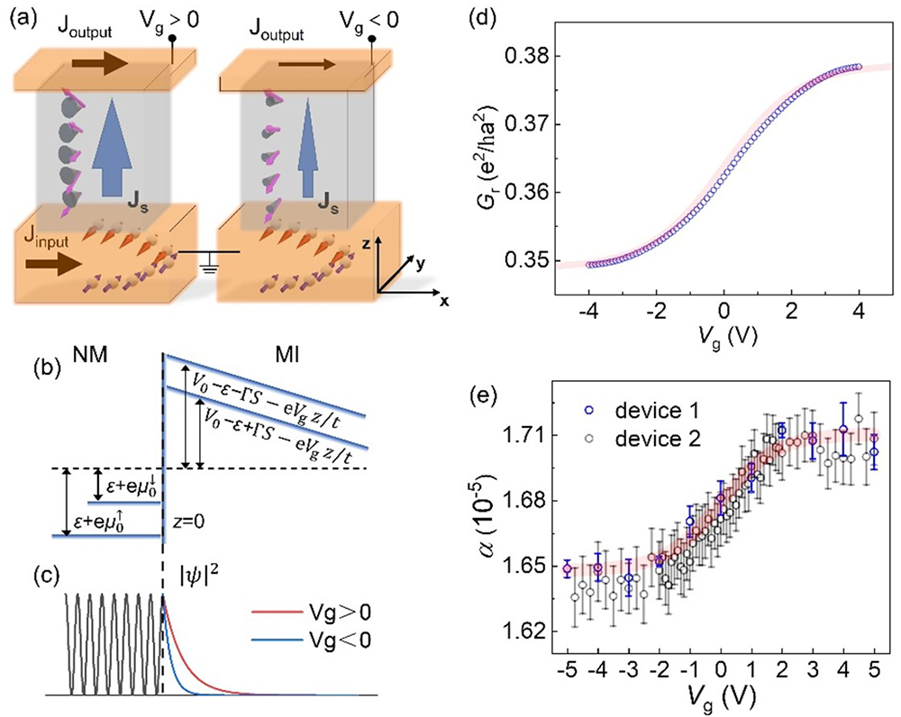
Figure 1. (a) Schematic diagram of the voltage-controlled magnon transistor. (b) Schematic diagram of the energy band at the bottom NM/MI interface under Vg > 0. (c) Schematic diagram of Vg controlled probability density of conduction electrons at the bottom NM/MI interface. (d) Numerically calculation results of Vg dependence of the real part of the spin-mixing conductance (Gr) at the bottom Pt/YIG interface and (e) experimentally measured Vg-controlled MECD efficiency (α) in Pt/YIG/Pt magnon transistor.
Contact:
Institute of Physics, Chinese Academy of Sciences
HAN Xiufeng
Email: xfhan@iphy.ac.cn
Key Words:
Magnonics; Voltage controlled magnon transistor; Interfacial exchange coupling.
Abstract:
Construction of voltage-controlled magnon transistors has posed a long-term challenge in the field of magnonics due to the charge neutrality of magnons. This study addresses this challenge by theoretically revealing the physical principles governing the voltage control of magnon flow and successfully fabricating a prototype voltage-controlled magnon transistor. The achievement of voltage control over magnon current was realized through the efficient control of spin-magnon conversion at the interface of nonmagnetic metal and magnetic insulator.